Logic Synthesis And Physical Implementation
Educational reference page converted from your Advanced Logic Synthesis and Physical Implementation source.
1. Logic Synthesis Fundamentals
Logical synthesis serves as the critical cornerstone of modern Very Large Scale Integration (VLSI) design. It acts as the definitive bridge translating a designer's abstract behavioral intent into a structurally equivalent, physical implementation. Within the conceptual framework of the Gajski-Kuhn Y-Chart, logic synthesis automates the traversal from the behavioral domain (what the circuit does) to the structural domain (how the circuit is built). The fundamental equation governing this domain is: Synthesis = Translation + Logic Optimization + Mapping .
1.1 Objectives and Optimization Goals
Synthesis is a constraint-driven optimization process. A synthesis engine explores a vast solution space to find a hardware structure that balances conflicting constraints. The primary goals dictate the parameters of the generated gate-level netlist:
- Performance (Timing): Achieving the target operating frequency by minimizing the delay of critical signal paths. This is measured by setup and hold slack. The tool resizes cells, restructures logic, and adjusts clock latencies to ensure all data paths meet the required clock period.
- Area Minimization: Reducing the total number of logic gates and their physical footprint, which directly correlates to manufacturing costs, silicon yield, and localized routing congestion.
- Power Reduction (DFP): Optimizing the design for both dynamic (switching) power and static (leakage) power consumption. This involves inserting specialized logic such as clock-gating cells or utilizing low-leakage threshold voltage (Vt) cells.
- Design for Testability (DFT): Automatically inserting test structures, such as scan chains and compression logic, to facilitate post-manufacturing defect testing. Synthesis tools must weave these test structures into the functional logic without disrupting functional timing or violating design rules.
- Logical Equivalence: The non-negotiable requirement that the final gate-level netlist is mathematically and functionally identical to the original Register-Transfer Level (RTL) description under all input conditions. Formal verification tools are utilized downstream to prove this equivalence.
1.2 Prerequisites and Synthesis Inputs
To successfully execute a synthesis run, a highly specific set of inputs must be prepared and loaded into the synthesis database. These inputs define both the functional behavior and the physical/electrical limitations of the target silicon.
- RTL Source Code: The functional behavior described in synthesizable subsets of Verilog, SystemVerilog, or VHDL. The coding style dictates the initial logic structures inferred by the tool.
- Technology Libraries (.lib, .db, .ndm): The ground truth for the synthesis tool, provided by the semiconductor foundry. These files contain detailed characterization data for every standard cell.
- Target Library: The primary standard cell library used for technology mapping, containing the physical gates (e.g., NAND, NOR, DFF).
- Link Library: Used to resolve references to instantiated cells, pre-compiled sub-modules, or memory macros.
- Synthetic Library: Contains complex, pre-optimized DesignWare components like adders, multipliers, and arithmetic logic units (ALUs).
- Design Constraints (SDC): Standardized scripts that establish the performance goals and electrical rules.
- Clocks: Defining the fundamental timing requirements, frequencies, and duty cycles.
- I/O Timing: Modeling external logic connected to the chip boundaries to account for input/output delays.
- Timing Exceptions: Explicitly telling the tool to ignore specific paths (false paths) or grant them multiple clock cycles, freeing up optimization resources for truly critical paths.
- Unified Power Format (UPF): An optional but critical input for modern low-power designs. It defines the power architecture, multiple voltage domains, power switches, level shifters, and isolation cells. Synthesis tools use this to enforce power intent physically.
- Floorplan Data (DEF): Design Exchange Format files providing physical placement data for macros, standard cell rows, and I/O pins. This enables the tool to estimate wire delays based on physical coordinates rather than relying purely on statistical Wire Load Models (WLM).
1.3 Sign-Off Criteria and QoR Metrics
The ultimate success of a synthesis run is judged against QoR metrics. Passing these metrics serves as the criteria for moving the design to the next stage (physical routing or final sign-off).
| Metric | Description |
|---|---|
| Setup Slack | The amount of time data arrives before the required setup window of a capturing register. |
| Hold Slack | The amount of time data remains stable after the active clock edge. |
| Total Negative Slack (TNS) | The cumulative sum of all negative slack across the design. Evaluates overall timing health and routing viability. |
| Worst Negative Slack (WNS) | The most severe timing violation in the design. Dictates the maximum achievable frequency. |
| Cell Area | Total physical silicon area consumed by standard cells, macros, and routing overhead. |
| Power Consumption | Estimated leakage and dynamic power based on annotated switching activity files (SAIF/VCD). |
| Design Rule Violations (DRC) | Checks for electrical viability such as maximum transition time, maximum fanout, and maximum capacitance. |
2. Core Optimizations
Before mapping the design to physical standard cells, synthesis tools perform technology-independent logic optimization on a generic representation of the circuit.
Optimization landscape: The chart organizes the major optimization families and shows how timing, area, and power objectives are balanced before and during mapping.
This figure shows synthesis as a closed optimization loop rather than a one-pass transform. The flow starts with structural cleanup, then repeatedly checks timing, area, power, and design-rule limits as mapping decisions evolve. Each loop changes the starting conditions for the next step, so QoR improves through convergence, not through a single isolated optimization.
2.1 Translation to Generic Boolean Logic (GTECH)
The synthesis engine first reads and parses the HDL files to check for syntax errors and build an intermediate hierarchical representation. The design is translated into a generic, technology-independent format known as GTECH.
- GTECH consists of idealized, unmapped logic primitives.
- This structural abstraction isolates the logic. It allows the tool to execute massive algebraic and Boolean transformations without being artificially constrained by the specific delay, area, or drive-strength penalties of a target foundry library.
- Complex RTL operators (like +, *, >>) are replaced with synthetic operators that act as placeholders until the datapath optimization engine selects the most appropriate hardware architecture.
2.2 Boundary Optimization and Constant Propagation
Boundary optimization involves the propagation of logic values across hierarchical module boundaries to simplify the overarching circuit and eliminate redundant logic.
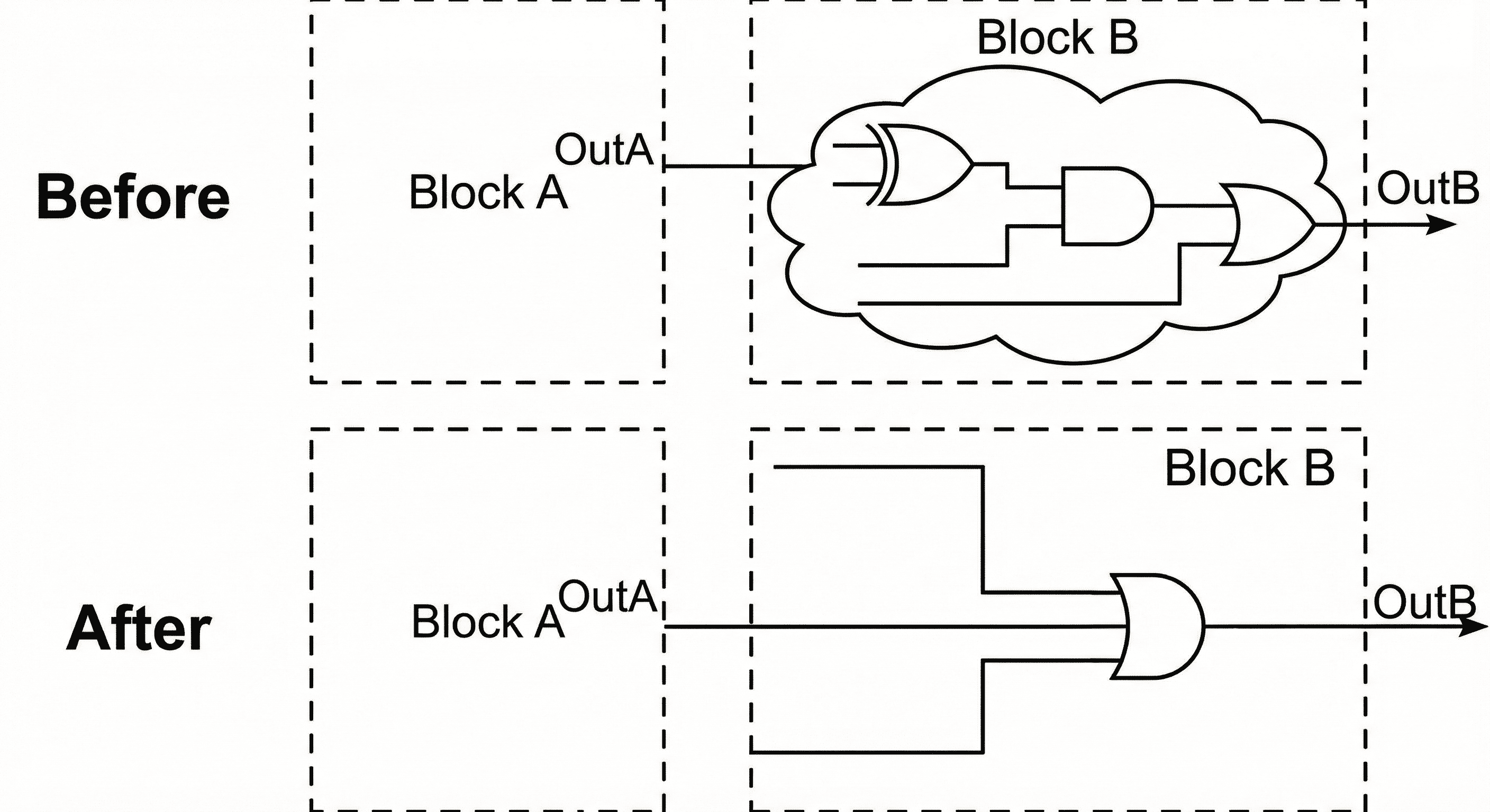
Constant propagation across hierarchy: When a hardcoded logic 0 is driven from Block A into Block B, downstream gates become mathematically deterministic and can be removed.
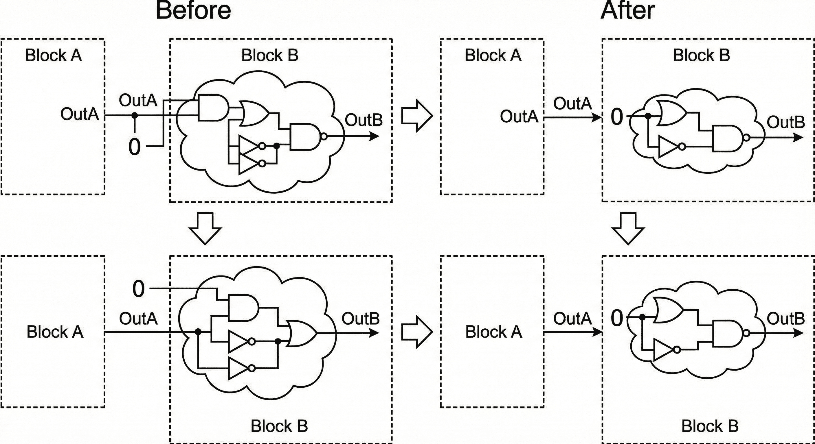
The diagram captures a common hierarchical case where one block drives a fixed logic value into the next block. Once that constant reaches the downstream cone, multiple gates become mathematically deterministic and can be simplified or removed without affecting outputs. The result is shorter logic depth, fewer switching nodes, and lower area because the cone is rebuilt around only the functionally active paths.
Phase inversion push: If inversion sits only at a hierarchy boundary, the tool can move it into the receiving cone so inversion can be absorbed or shared by downstream gates.
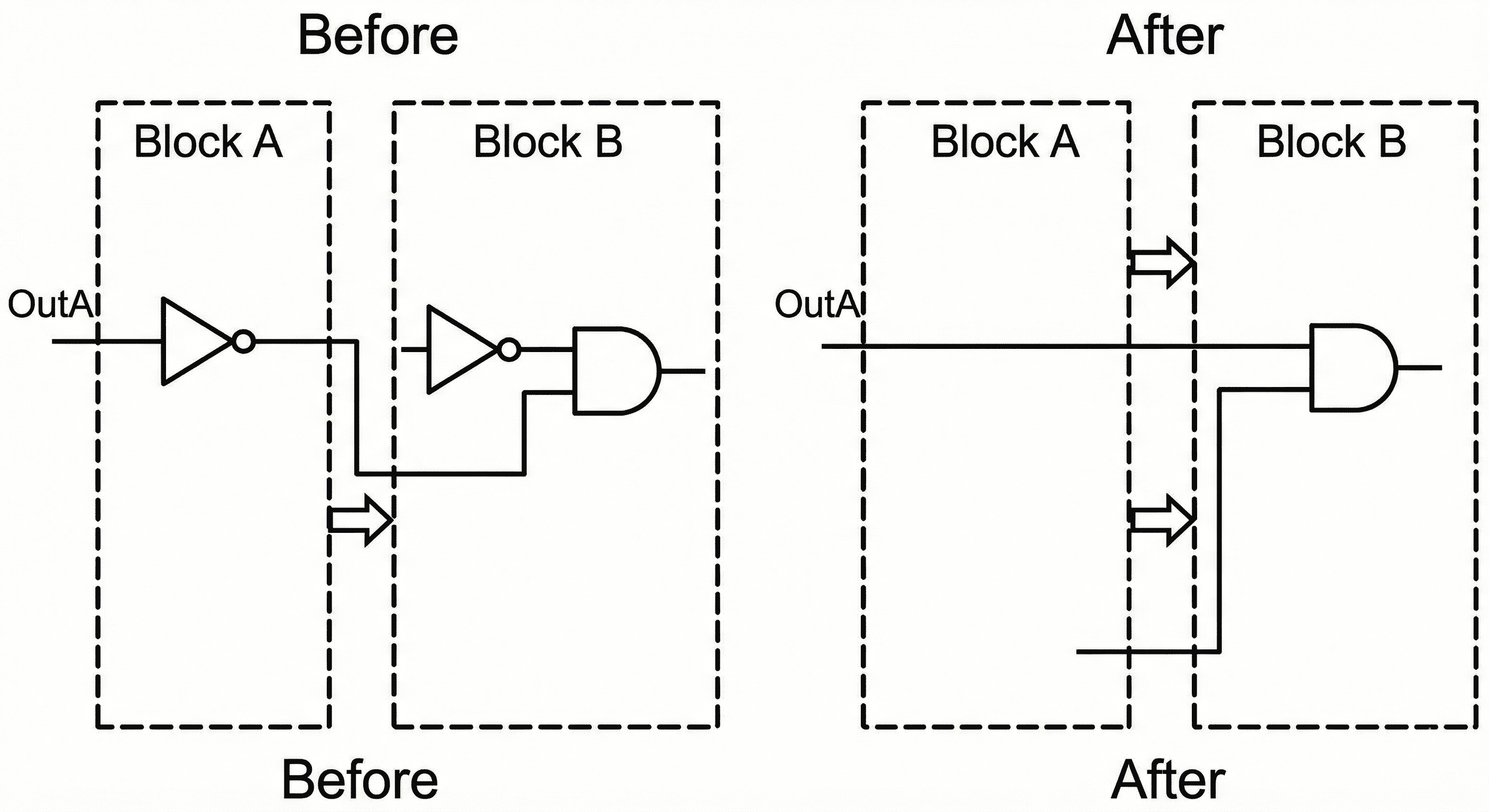
This transformation moves inversion across module boundaries so the same Boolean meaning is preserved while the internal cone becomes easier to optimize. After inversion is pushed inward, the tool can absorb polarity into NAND/NOR structures, merge equivalent terms, and reduce standalone inverter count. That improves both delay and area because redundant polarity conversions are eliminated from the active path.
Unloaded logic removal: If a logic cone has no valid fanout endpoint, it is dead code and should be removed. Equal-opposite logic propagation also merges equivalent or inverted-equivalent nets.
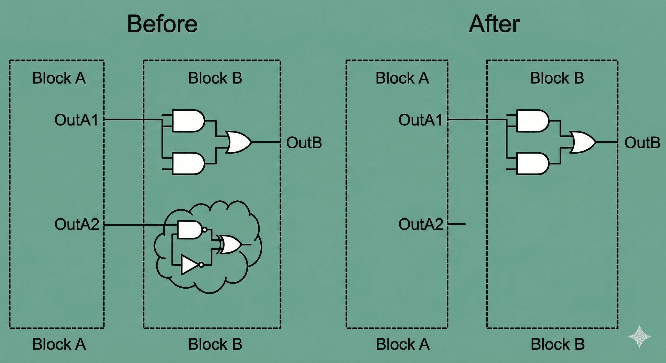
Here the removed logic cone has no observable fanout at chip outputs or state elements, so it contributes no functional behavior. Keeping it would still consume gates, routing tracks, and internal toggling energy during simulation activity. Pruning this cone recovers silicon resources and reduces dynamic power while preserving exact functional equivalence of all visible outputs.
2.3 Hierarchy Management
By default, logical hierarchies defined in the RTL are preserved to maintain human readability and modularity. However, rigid boundaries act as walls that restrict optimization algorithms.
- Ungrouping (Flattening): The tool automatically dissolves hierarchical boundaries (via automatic ungrouping mechanisms), merging sub-designs into their parent modules. This dramatically expands the optimization scope, allowing the tool to share common sub-expressions and reduce logic depth on critical paths that previously crossed boundaries.
- Preservation: Designers can apply attributes to explicitly preserve specific hierarchies. This is mandatory for modules adhering to strict UPF power domains, physical macros, or third-party intellectual property (IP) blocks that must not be altered.
2.4 Datapath and MUX Optimization
Datapath optimization specifically targets arithmetic operators (addition, subtraction, multiplication, shifting) and combinational logic paths to improve timing and area.
Arithmetic datapath extraction: A + B + C + D implemented as cascaded carry-propagate adders creates a long linear bottleneck. A carry-save architecture compresses operands in parallel and postpones carry combination to a later stage.
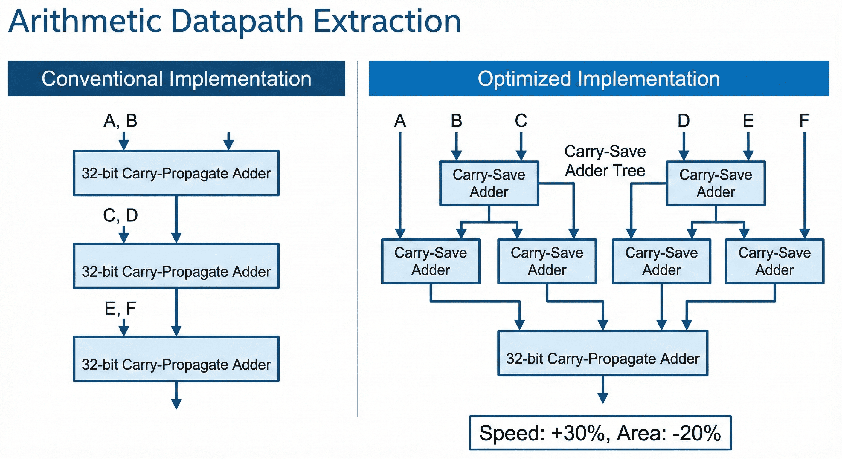
The image shows a transition from serial carry propagation to carry-save compression across multiple operands. Instead of waiting for each carry to settle stage by stage, partial sums and carries are generated in parallel and only resolved in a final stage. This shortens the critical arithmetic path and gives the placer/router a more balanced timing structure for wide datapaths.
Data-path reshaping: Deep serial combinational chains are restructured to reduce logic depth, while critical cells are selectively resized to improve propagation on constrained paths.
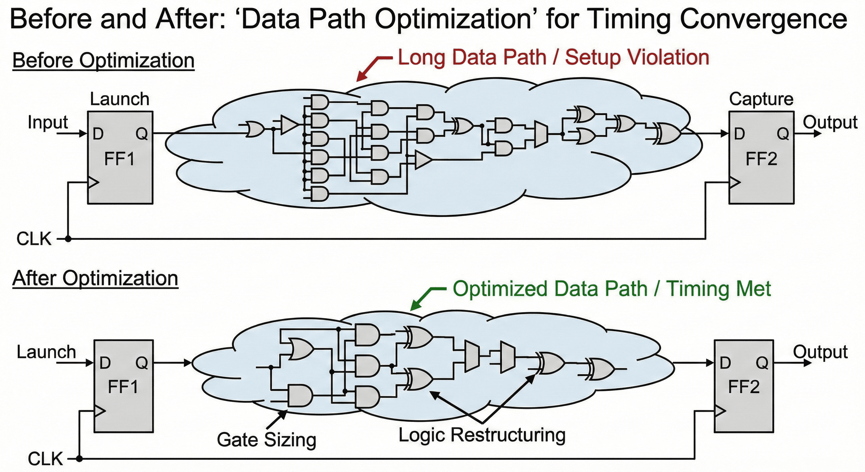
This scenario illustrates selective datapath tuning where only true setup-limited arcs are restructured or resized. Non-critical branches are intentionally left stable so the design does not pay unnecessary area and leakage cost for blanket optimizations. The payoff is targeted timing recovery with better overall QoR balance across timing, area, and power.
MUX intent mapping: Selection behavior built from generic AND/OR/NOT logic is recognized and mapped to dedicated multiplexer cells from the technology library.
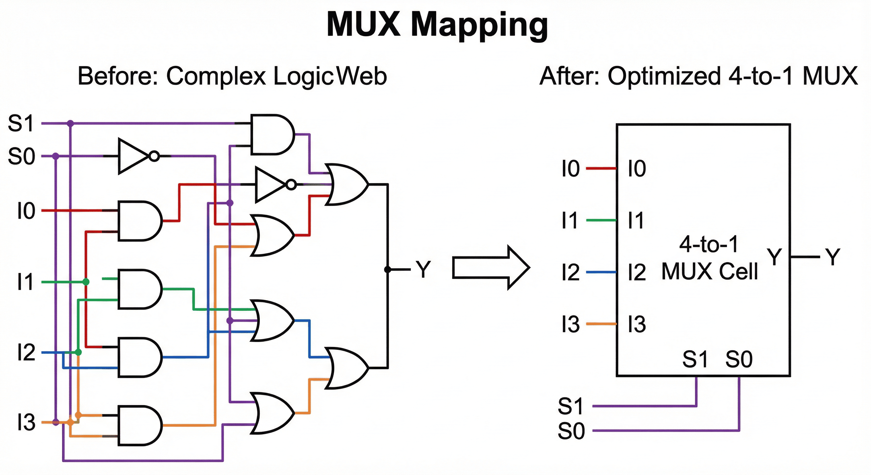
The before/after structure shows generic gate networks being recognized as multiplexing intent and then remapped into dedicated mux cells. Native mux cells use transistor topology optimized for select-path delay, pin capacitance, and compact footprint compared with decomposed AND/OR/INV trees. Mapping this intent early improves both timing predictability and placement density in control-heavy logic.
2.5 Sequential Mapping and DFT
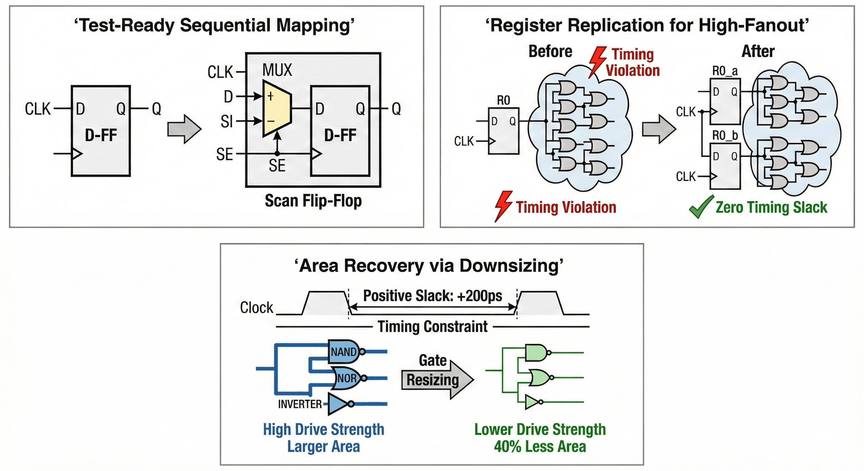
Core Target: To enable post-manufacturing silicon testing without degrading functional timing or area targets unnecessarily. During the initial synthesis mapping, the engine prepares the design for automated test equipment (ATE) by modifying the sequential elements. The tool systematically identifies standard registers inferred from the RTL and replaces them with scan-equivalent library cells. This ensures that the physical layout tools can stitch these registers into long "scan chains" later in the flow, allowing test patterns to be shifted in and out of the chip to identify manufacturing defects.
Scan-aware replacement behavior: Functional data capture is preserved, and additional scan control pins are introduced so the same state elements can operate in functional mode and test-shift mode.

This flow tracks how a functional DFF is replaced by a scan-capable cell while preserving functional behavior in mission mode. The scan-enable path multiplexes between normal data and serial scan input so internal states become controllable and observable during manufacturing test. The value is high test coverage without redesigning RTL functionality, with timing impact managed during later optimization passes.
- Before Mapping: A standard D-Flip-Flop (D-FF) receives a clock (CLK) and a data input (D), outputting the functional data (Q).
- After Mapping: The tool replaces it with a "Scan Flip-Flop." This cell incorporates an integrated multiplexer (MUX) directly on the input. During normal operation, the Scan Enable (SE) pin is low, and functional data (D) passes through. During test mode, the SE pin is driven high, allowing the alternative test pattern signal (Scan In or SI) to be shifted serially through the register. By integrating this MUX directly into the standard cell rather than building it out of discrete logic gates, the synthesis tool minimizes the delay penalty added to the critical functional data path.
2.6 Register Replication
Core Target: Resolve setup timing violations and electrical design rule (DRC) violations caused by excessive capacitive loading on high-fanout nets. When a single register drives a massive number of endpoints (a high-fanout net), the immense capacitive load severely slows down the signal's transition time. This sluggish transition eats into the available clock cycle, causing downstream setup timing violations. While traditional High-Fanout Net Synthesis (HFNS) attempts to fix this by inserting a deep tree of buffer cells, buffer trees inherently add their own insertion delay. An often superior timing optimization is Register Replication . The synthesis tool duplicates the driving register and geographically partitions the fanout loads among the new clones. This slashes the capacitive load on each individual output pin, accelerating the signal transition and resolving the setup timing crisis without adding buffer layers.
Load partitioning behavior: Register clones divide sink groups so each driver sees lower capacitance and cleaner transition behavior.

The figure starts with one register driving excessive fanout, which creates heavy capacitive loading and slow transition edges. Replication splits sinks across cloned registers so each output drives a smaller load, improving slew and reducing delay variability. This is especially effective when high-fanout control nets block setup closure on multiple endpoint groups.
- Before Optimization: A single source register (RO) drives a massive combinational logic cloud consisting of numerous gates. The heavy capacitive load causes a slow transition, resulting in a "Timing Violation" (indicated by the red lightning bolt).
- After Optimization: The tool executes register replication, cloning the source register into two identical, parallel registers (RO_a and RO_b). The logic cloud is split in half, with each new register driving only a portion of the original load. This effectively halves the capacitive delay, successfully driving the slack to a "Zero Timing Slack" (or positive) margin (indicated by the green checkmark).
2.7 Area Recovery and Gate Downsizing
Core Target: Reclaim physical silicon area and reduce static leakage power on non-critical timing paths. Logic synthesis is a continuous, dynamic tradeoff between speed, area, and power. During the initial timing-driven mapping phases, the synthesis engine aggressively up-sizes standard cells (choosing high-drive-strength, large-area gates) to guarantee that all setup timing constraints are met. However, this often results in non-critical paths being far faster than necessary, wasting area and leaking power. Area Recovery is a specialized pass where the tool analyzes the timing graph to identify paths with an excess of positive slack. It then deliberately scales back the logic on those paths, swapping the large, fast gates for smaller, slower, and less power-hungry variants.
Slack-to-area tradeoff behavior: Surplus timing margin is intentionally consumed so cell sizes can be reduced while preserving timing legality.

This chart captures a guarded tradeoff: cells with healthy positive slack are candidates for lower drive strength, while timing-sensitive cells remain protected. The optimization intentionally converts excess margin into reduced cell area and leakage current, then rechecks setup and hold to prevent regressions. It is a recovery step after timing closure, not a random size reduction across the netlist.
- Before Optimization: A timing path driven by high-drive-strength NAND, NOR, and INVERTER gates completes its computation well before the clock edge, leaving a comfortable "Positive Slack: +200ps" margin against the timing constraint.
- After Optimization: Recognizing the wasted margin, the tool performs "Gate Resizing." It swaps the "High Drive Strength / Larger Area" gates for "Lower Drive Strength" equivalents. This reclaims up to "40% Less Area" per cell and significantly cuts static leakage power, all while perfectly absorbing the 200ps margin and keeping the path strictly within the required timing constraints.
2.8 Register Merging
Core Target: Reduce area and dynamic/static power by eliminating logical redundancy in sequential elements. While register replication duplicates registers to fix timing, Register Merging does the exact opposite to save area and power. During synthesis, the tool actively scans the design for logical redundancy. If it identifies multiple individual registers that are strictly equivalent-meaning they receive the exact same data input and share the exact same clock and control signals-it automatically merges them into a single physical register. The tool deletes the redundant duplicates, and the single surviving register takes over driving all of the downstream loads. It is important to clearly distinguish this from Multibit Banking. While banking physically groups distinct data bits (that happen to share control logic) into a shared macro footprint, register merging entirely eliminates the duplicate data paths from the netlist, resulting in a direct, absolute reduction in total gate count and switching power.
Equivalence-driven merge behavior: Only sequential elements with identical data/control semantics are merged, so function is preserved while redundant state hardware is removed.

The merge path begins when two sequential elements are proven equivalent in data, clock, reset, and enable behavior. One register is removed and fanouts are reconnected to the survivor, reducing sequential cell count and local routing complexity. Because equivalence is validated before rewiring, the transformation cuts area and clocked switching load without altering cycle-accurate behavior.
3. Unified Physical Synthesis Flow
Traditional logic synthesis relied on statistical Wire Load Models (WLM) to estimate interconnect delay. However, at advanced semiconductor nodes (sub-16nm), wire resistance and capacitance dominate cell delays, rendering WLMs wildly inaccurate. To resolve this, modern synthesis tools employ Unified Physical Synthesis, which tightly integrates placement, congestion analysis, and routing engines directly into the synthesis pipeline.
3.1 Physical Synthesis Paradigm
The core physical synthesis engine acts as the central driver for unified physical synthesis, replacing legacy wire-load-based compilation paradigms. It executes a sequence of highly deterministic, physically-aware stages.
Stage-by-stage pipeline: The unified flow progresses from logical mapping to physically correlated optimization in a single continuous engine.
- 1. RTL & Constraints Entry: The foundational step where the raw RTL (Verilog/VHDL) and physical/timing constraints (SDC, UPF, DEF) are loaded into the database.
- 2. Logic Mapping (GTECH): The tool translates the RTL into generic Boolean logic (GTECH) and maps it to the target standard cell library. This corresponds to the initial mapping and logic optimization phases, focusing on area reduction and technology-dependent delay optimization.
- 3. Initial Placement & Congestion Analysis: Corresponds to the initial placement phase. The tool performs a coarse, global placement of all mapped cells onto the floorplan. It merges clock-gating logic and generates a congestion map to identify routing bottlenecks early in the flow.
- 4. Electrical DRC Fixing: Corresponds to the initial electrical design rule check phase. The tool analyzes the physical distances between placed cells and builds high-fanout-net synthesis (HFNS) trees. It inserts buffers to fix severe electrical Design Rule Check (DRC) violations, such as maximum capacitance and maximum transition time violations.
- 5. Physical Optimization (Sizing/Buffering): Corresponds to the physical optimization and final placement phases. The tool iteratively resizes cells and restructures logic based on actual physical distances and routing estimates, moving cells to alleviate congestion and improve timing correlation.
- 6. CCD (Concurrent Clock-Data) Optimization: A specialized phase where the tool simultaneously optimizes clock tree latencies (intentional skew) and data path logic to close complex timing violations that cannot be fixed by data path sizing alone.
- 7. Handoff to PnR: The final output is a physically optimized, legally placed, and legally routed (globally) gate-level netlist, ready for handoff to the detailed Place and Route (PnR) engines.
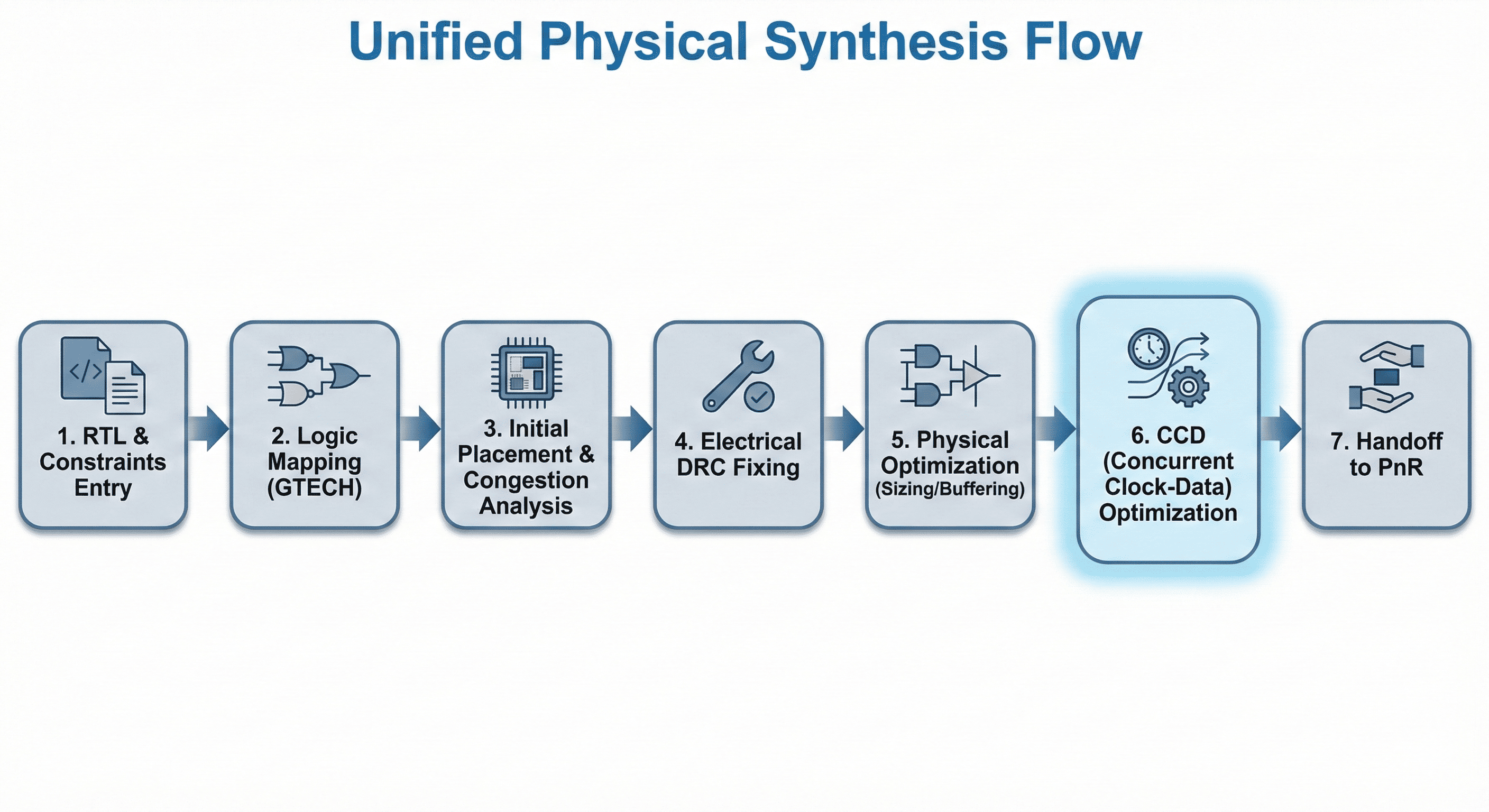
This flow makes clear that modern synthesis quality depends on physical awareness from the earliest stages. Netlist choices are evaluated with placement estimates, congestion feedback, and extracted electrical context instead of idealized wire assumptions. That early correlation reduces late-stage surprises, shortens closure loops, and produces a handoff netlist that is much closer to final routed behavior.
3.2 Prechecks and Early Data Handling
Before initiating heavy optimization algorithms, the environment utilizes an Early Data Check mechanism. This validates the integrity of the design inputs to prevent catastrophic, computationally expensive late-stage failures.
- Missing Information Check: Validates the presence of scan definitions (for testability), floorplan parameters, site rows, and routing tracks.
- Mismatch Mitigation: Ensures consistency between the logical netlist and the UPF power intent. Any conflict between the RTL definition and the physical power domains is flagged as a multivoltage design check error.
4. Concurrent Clock and Data (CCD) Optimization
In traditional ASIC design flows, clock networks are synthesized to have zero skew-meaning the clock signal is engineered to arrive at every register in the design at exactly the same time. However, enforcing zero skew strictly limits the maximum operating frequency of a chip if the combinational data paths between registers are imbalanced.
4.1 Useful Skew and Slack Balancing
Concurrent Clock and Data (CCD) optimization discards the zero-skew paradigm in favor of Useful Skew . CCD intentionally adjusts the clock arrival times (clock latencies) at specific registers to "borrow" or "steal" time from a path with positive slack and donate it to an adjacent path with negative slack.
Useful-skew timing shift: In failing cases, the capture edge can be delayed so late-arriving data gains enough time to satisfy setup at the destination register.
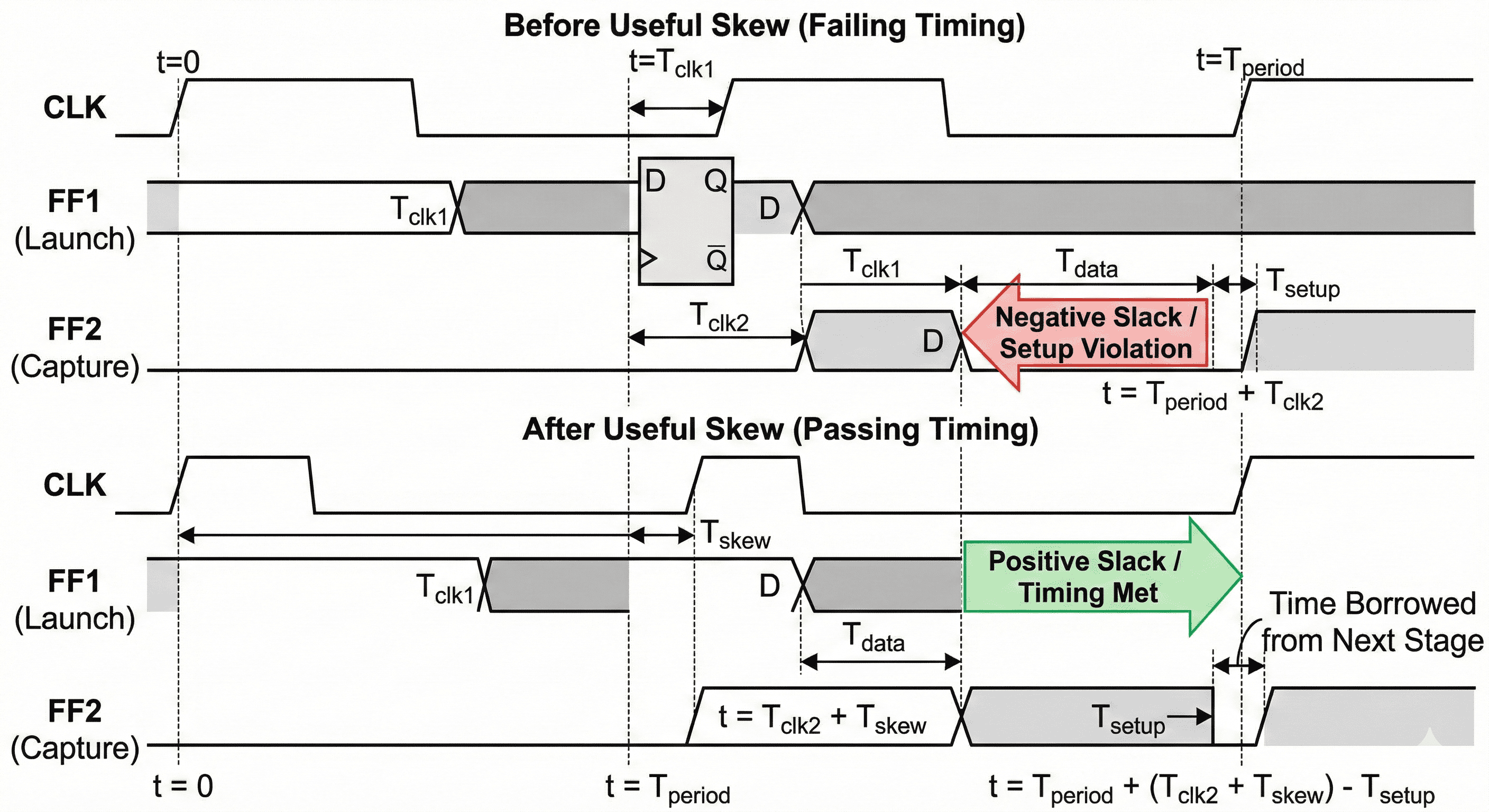
The timing windows in this image show how capture and launch relationships are intentionally shifted to donate time where setup is failing. Useful skew is applied with bounds so hold margins on adjacent short paths are not accidentally broken. The method improves worst paths by redistributing existing margin across the clock network rather than only pushing data-path upsizing.
Clock-path tuning for launch/capture balance: Buffer sizing and insertion-delay control can move launch or capture timing to align with real datapath delay.
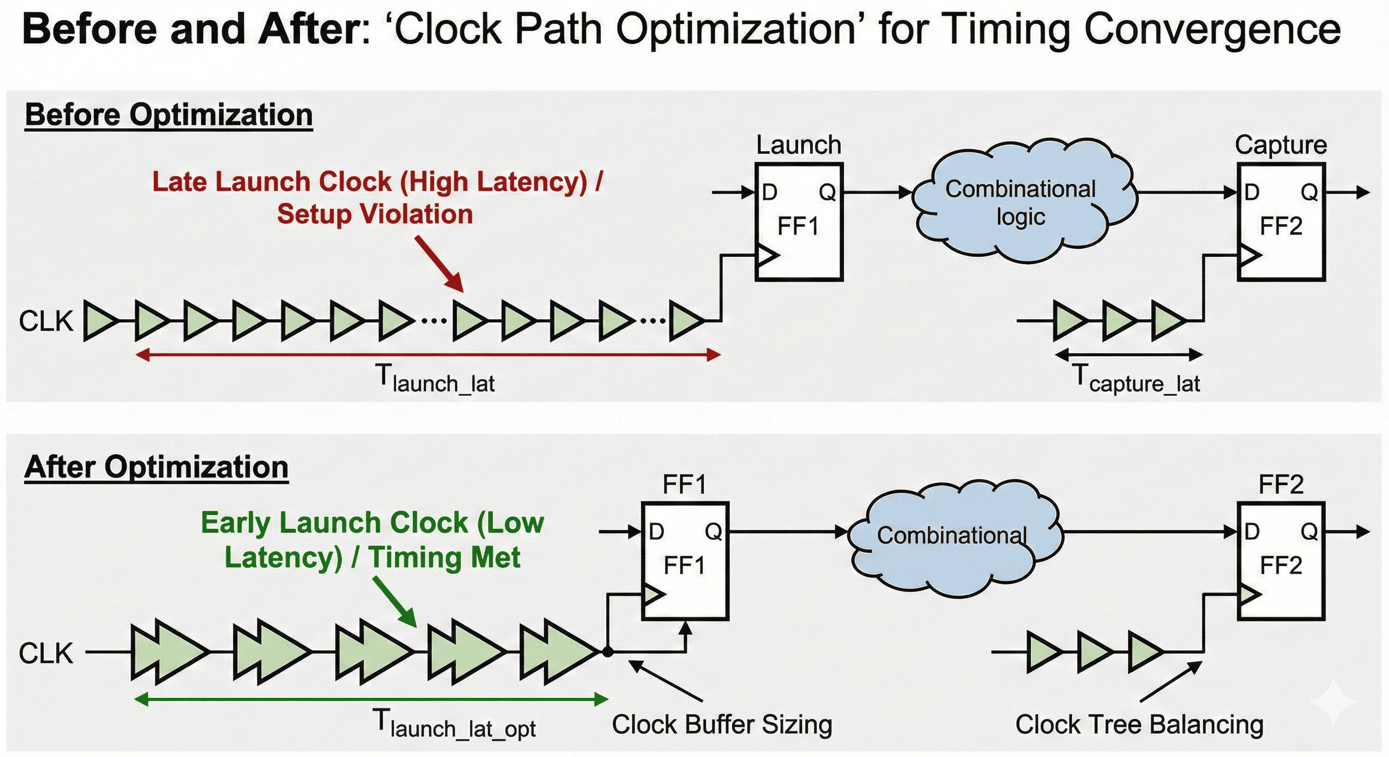
The clock-tree view highlights localized latency tuning through buffer sizing, insertion, and branch-level balancing. Instead of perturbing the entire tree, adjustments are focused on sinks that participate in violating paths, preserving stability for unaffected domains. This targeted clock shaping increases effective data travel time where needed while keeping skew and insertion-delay constraints controlled.
Joint clock-data optimization: The most robust closure comes when skew edits and datapath restructuring are solved together rather than in isolation.
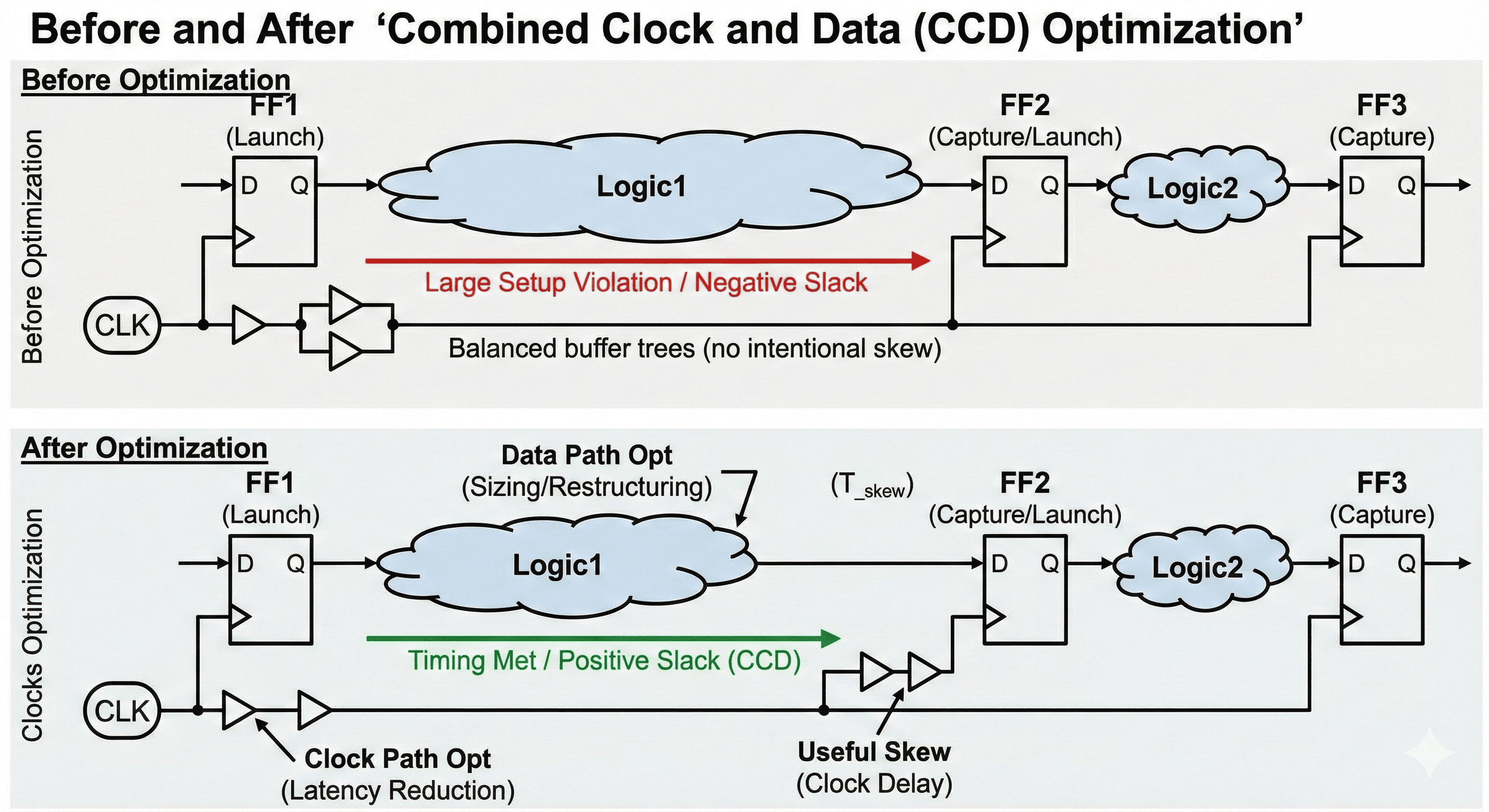
This diagram explains why CCD is more effective than isolated data-path fixes on advanced nodes. Clock adjustments and logic restructuring are solved together so each action is evaluated against the other in the same iteration. The coupled approach reduces ping-pong behavior between CTS and logic optimization and converges faster on legal setup/hold closure.
4.2 CCD Flow
Within advanced unified synthesis tools, CCD is tightly integrated into the preroute synthesis, clock tree synthesis, and postroute stages.
- Latency Limits: To prevent the tool from skewing clocks to unstable extremes (which could cause catastrophic hold-time failures), designers specify rigid limits. Tool constraints dictate the maximum limit on how early a clock can arrive and how late a clock can arrive.
- Boundary Path Exclusion: Clock signals driving input/output boundary registers interface with external components whose timing cannot be internally skewed. Designers can use boundary timing exclusion constraints to restrict CCD solely to internal register-to-register paths, ensuring external I/O protocols are not violated.
- Data Path Aware (DPA) CUS: Compute Useful Skew (CUS) evaluates the power potential of a datapath. If a path can be downsized to save power but currently has zero slack, DPA-CUS deliberately shifts clock arrival times to artificially create positive slack on that path. The optimizer then aggressively downsizes the logic cells, trading the newly created slack for reduced leakage and dynamic power.
- Targeted Optimization: During postroute optimization, CCD can be constrained to operate exclusively on the most critically failing endpoints (e.g., the worst timing paths) via targeted endpoint optimization constraints. This prevents widespread, unnecessary perturbation of an already legally routed clock tree.
4.3 Machine Learning in CCD and RDE
To bridge the correlation gap between pre-route synthesis and post-route sign-off, synthesis engines utilize Route-Driven Estimation (RDE) combined with Machine Learning (ML). The tool extracts physical features during clock tree synthesis and trains an algorithmic model against actual labels generated after detail routing. In subsequent iterations, machine learning predictors accurately forecast post-route timing delays and voltage drops during the preroute CCD phase, leading to highly convergent, predictable silicon.
5. Multibit Banking and Debanking
As process nodes shrink, the clock distribution network consumes an increasingly disproportionate amount of a chip's total dynamic power and routing resources. Multibit optimization directly addresses this by combining multiple single-bit flip-flops into a single physical multi-bit cell.
5.1 Multibit Banking Benefits
A standard 1-bit flip-flop requires its own clock input pin, data input pin, data output pin, and often a reset pin. If a 32-bit bus requires 32 flip-flops, the clock tree router must branch the clock signal 32 times, adding significant wire length, via resistance, and buffer capacitance. By mapping these to 4-bit or 8-bit Multibit Flip-Flops (MBFF), the registers share a single set of internal clock and reset inverters.
- Power Reduction: The total capacitance of the clock tree is drastically reduced because there are far fewer physical clock sinks to drive.
- Area Optimization: Shared internal transistors for clock and reset buffering reduce the overall silicon footprint compared to individual discrete cells.
- Routing Congestion Relief: Fewer pins mean fewer local routing wires, freeing up critical metal tracks for dense datapath routing.
5.2 RTL Inference to Physical Mapping
The Multibit Banking process requires seamless coordination between the RTL parser and the physical placement engine.
Optimization loop control: Banking is applied when legal and beneficial, then re-evaluated during placement and routing. Debanking is triggered only where local closure quality degrades.
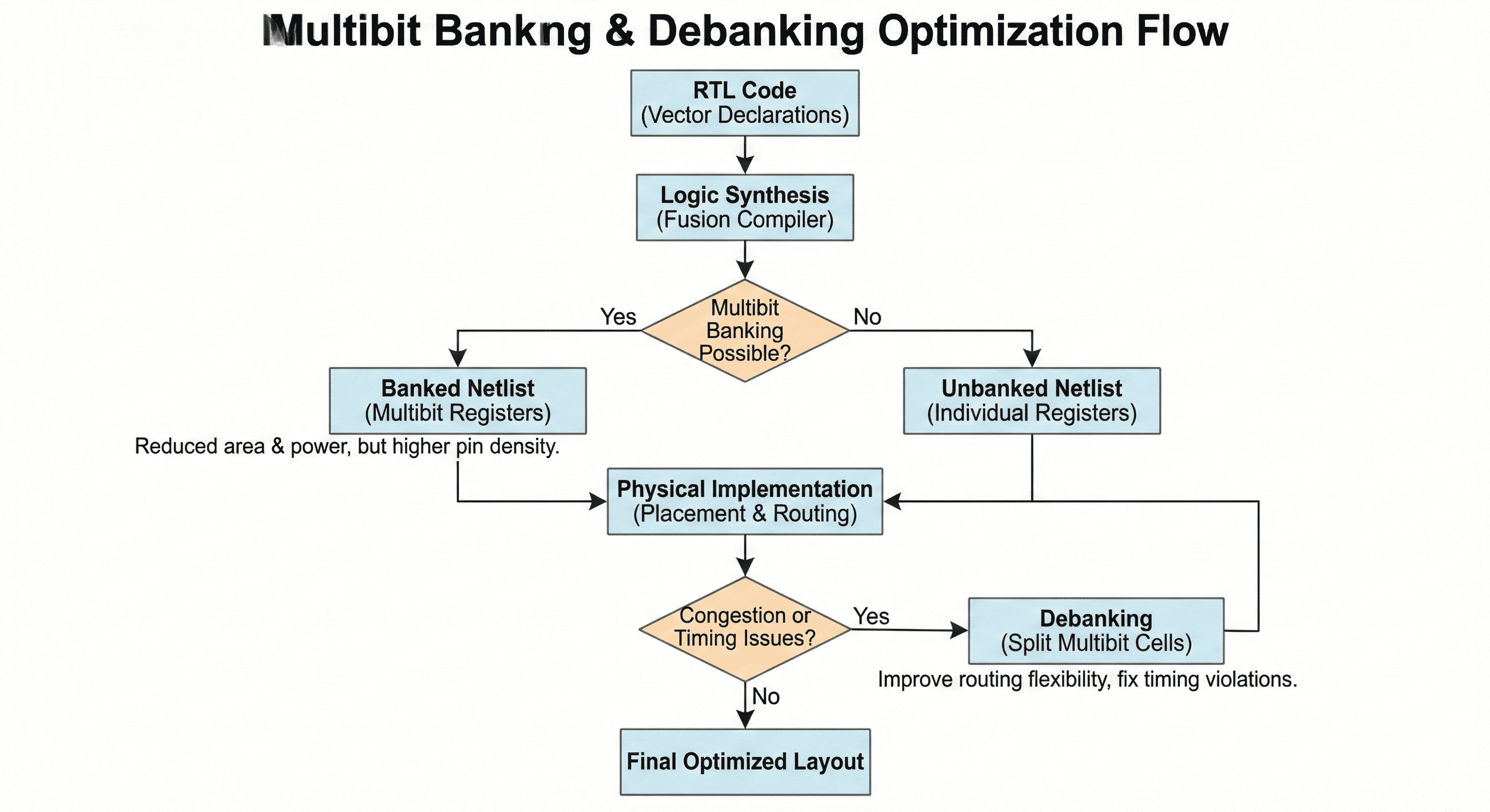
The sequence in this flow starts with candidate grouping, then validates each banking decision against timing, congestion, pin access, and placement legality. When a bank degrades local QoR, the loop triggers selective debanking so only problematic bits are split back out. This closed-loop behavior is important because the best power structure is often not the same as the best physical implementation structure in every region.
Physical banking of single-bit registers: Four 1-bit DFFs are mapped to one MBIT register so clock/reset hardware is shared.
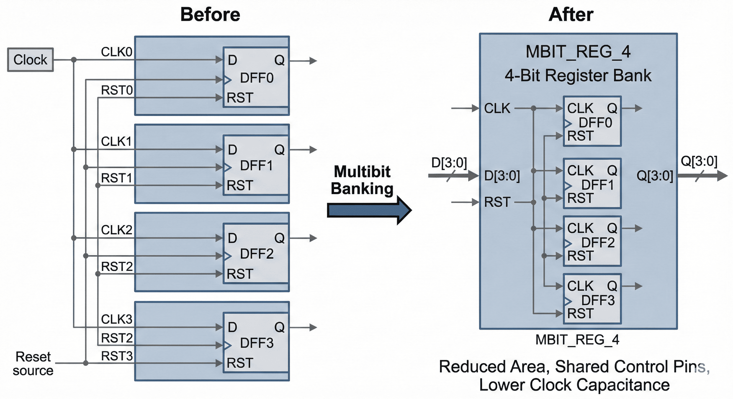
This figure shows how multiple single-bit flops are physically replaced by a multibit register with shared clock and control circuitry. Sharing those internal drivers reduces total pin capacitance and cuts redundant transistors, which directly lowers clock-tree switching power. It also frees routing channels because fewer control connections need to be distributed at the cell boundary.
Inference from RTL vectors: Vectorized RTL declarations (such as reg [3:0]) allow early inference of multibit cells during mapping.
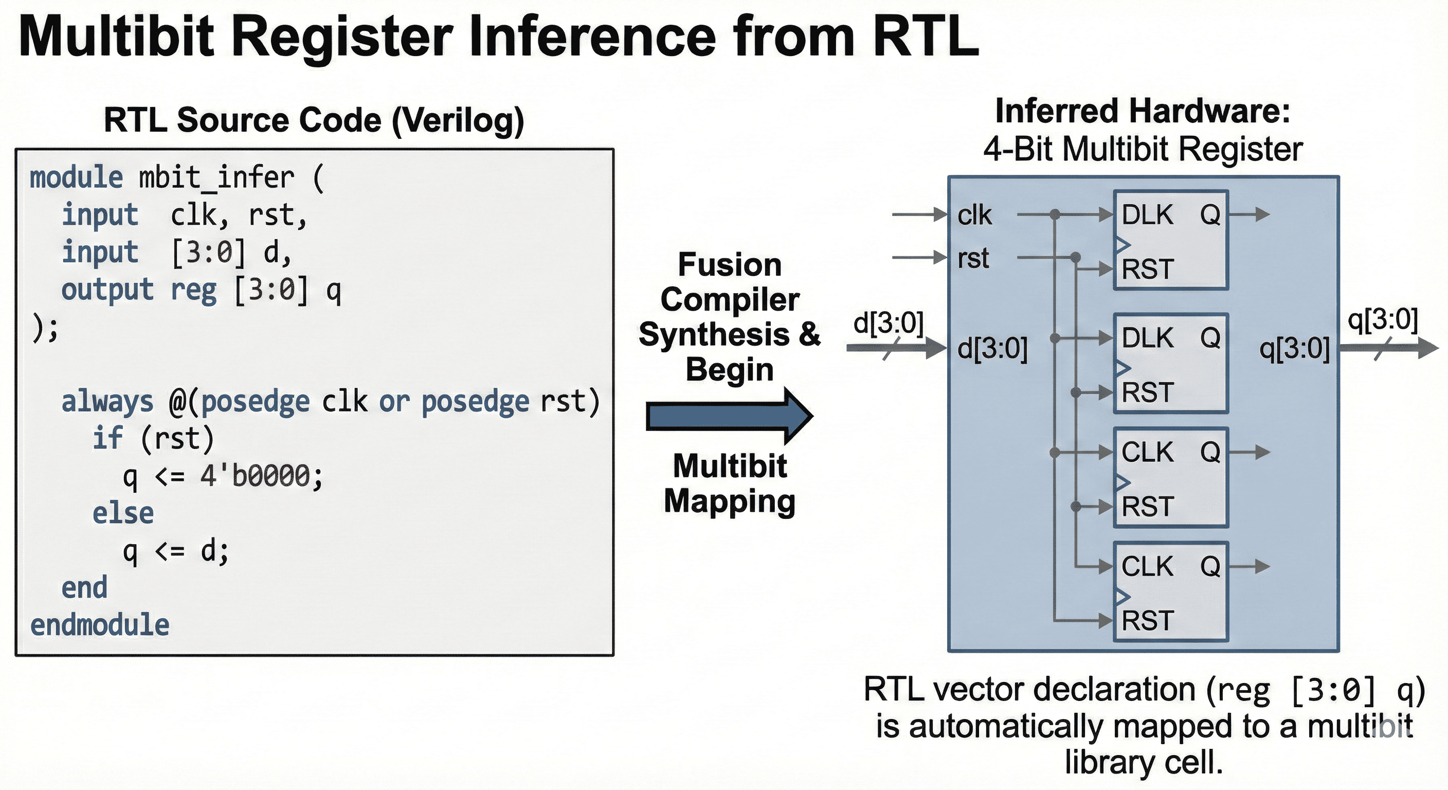
The RTL-centric view explains that vectorized register intent can be inferred before full physical mapping. Early recognition allows synthesis to carry multibit candidates through optimization instead of reconstructing intent late after logic has fragmented. This improves consistency between RTL structure and implementation and enables earlier power and area gains with less rework downstream.
Debanking for local recovery: If a banked cell causes localized congestion or endpoint detours, the tool can split it back into individual flops.
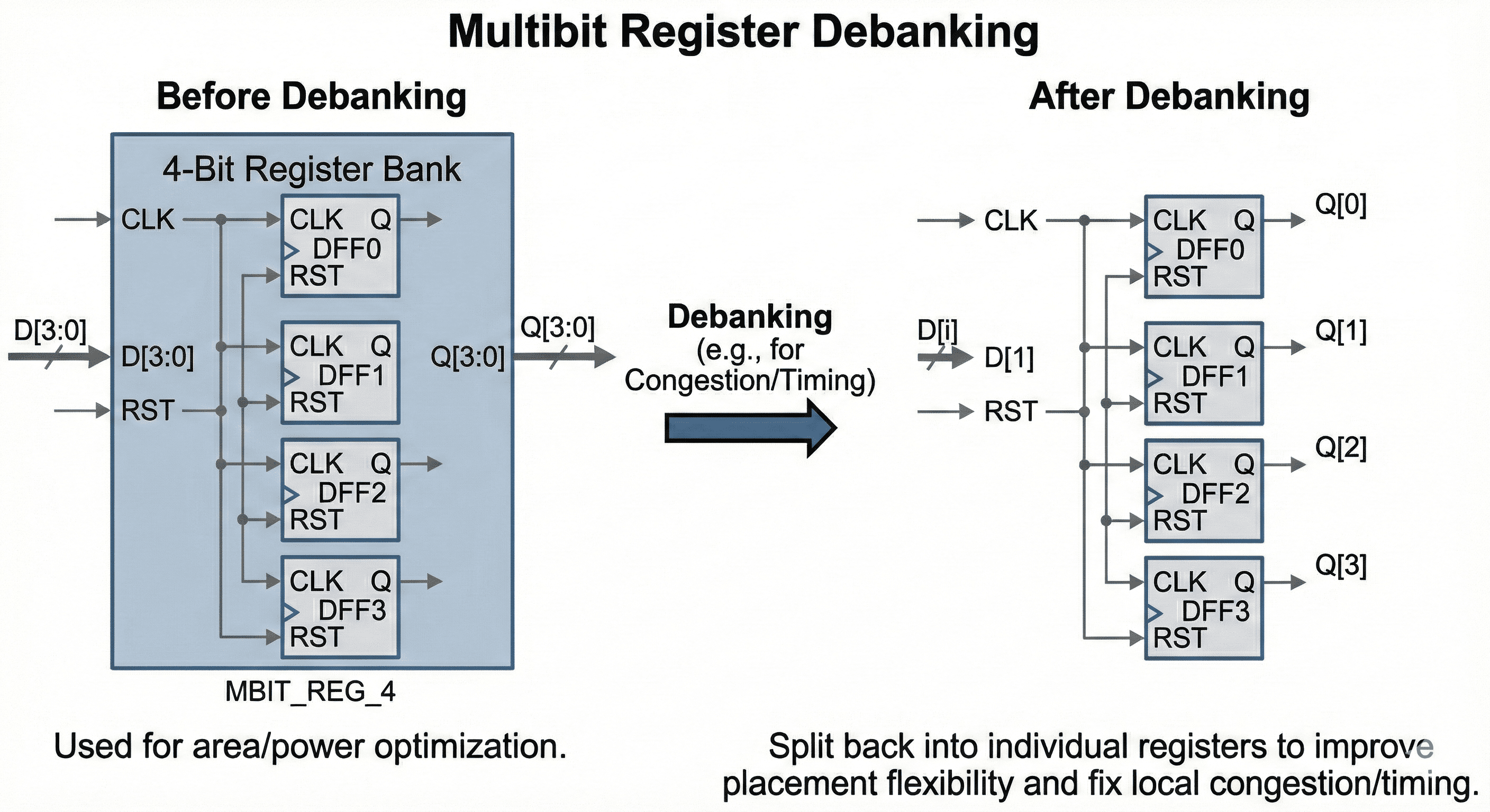
This image captures the corrective step where a previously banked group is split in only the congested or timing-sensitive region. Debanking restores placement freedom, shortens detoured routes, and can recover hold/setup margins that were lost due to over-constrained clustering. Applying it selectively protects most multibit power benefit while removing local closure blockers.
5.3 Multibit Flow Controls
In modern physical synthesis, multibit optimization is a highly dynamic process governed by strict timing and physical considerations.
- RTL Banking (Initial Mapping Phase): Groups registers logically before placement. To ensure that testability scan chains are not broken improperly, the tool executes strict scan chain checks prior to banking.
- Physical Banking (Physical Optimization / Final Placement Phases): Registers that were not grouped at the RTL stage can be banked based on physical proximity. If the placer puts two compatible 1-bit registers adjacent to one another to satisfy data flow, the physical banking engine swaps them for a 2-bit MBFF to save power without violating placement legality.
- Control Settings: Designers use specific constraints to strictly govern multibit configuration.
- Exclusion: Specific critical registers can be excluded entirely to preserve strict timing.
- Naming Styles: To maintain verification traceability, the tool manages complex hierarchical names using compact hierarchical naming controls to compress resulting instance names, preventing unreadable, bloated netlist nomenclature.
- Cross-Probing: Formal verification tools require structural mapping files. Every time the engine banks or debanks a register, it records the structural transformation to prove mathematically that the multibit configuration remains logically equivalent to the RTL definition.
6. SAIF-Driven Power and Clock Gating
With the undeniable shift toward mobile, edge computing, and high-density AI accelerators, power consumption dictates a chip's physical viability. Logic synthesis actively optimizes dynamic and static power profiles driven by highly accurate switching data.
Power-closure loop: Dynamic and static optimizations are evaluated together and accepted only when timing remains valid.
- Dynamic Power: The tool attacks active switching power by inserting Integrated Clock Gating (ICG) to stop unnecessary toggling, and by applying Multibit Banking to drastically reduce the clock tree wire length and capacitance.
- Static Power: The tool attacks leakage current by utilizing Multi-Vt Mapping (swapping fast, leaky cells for slower, low-leakage cells on non-critical paths) and performing Gate Downsizing (reducing cell sizes where timing permits).
- Timing Verification: Both power reduction branches continuously feed into a "Timing Verification" step to ensure that the aggressive power optimizations do not create new timing violations, establishing a closed-loop optimization cycle.
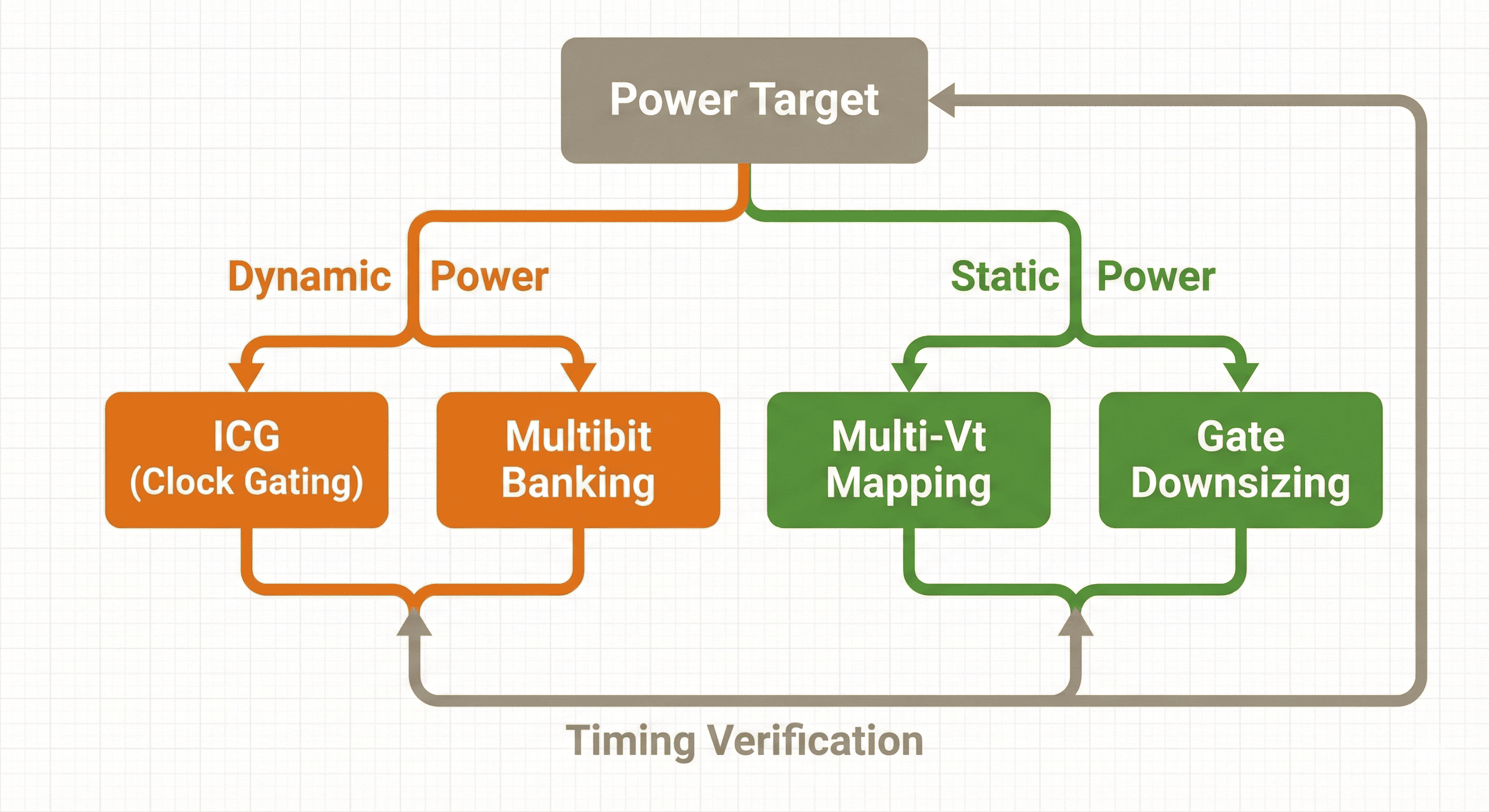
The power loop in this figure begins with activity-driven hotspots, applies structural changes, and then immediately rechecks timing and design rules. Some low-power transforms reduce slack or worsen transitions, so the loop keeps only those that remain electrically and temporally legal. This is why practical power closure is iterative and metrics-driven, not a single pass of power-only edits.
6.1 Switching Activity and SAIF Integration
Dynamic power is mathematically defined by the formula: , where is capacitance, is voltage, is frequency, and is the switching activity (toggle density). To optimize , verification engineers simulate the RTL using real-world software workloads to generate a Switching Activity Interchange Format (SAIF) file. SAIF is vastly superior to the older Value Change Dump (VCD) format for power estimation because it records cumulative signal statistics (static probability and toggle density) rather than logging every temporal value change, keeping file sizes manageable and compilation times fast.
Threshold-assignment strategy: Fast low-Vt cells are reserved for truly critical paths, while high-Vt cells are used where slack exists to cut leakage.
- Before Optimization: A logic cloud heavily utilizes a uniform threshold voltage (Standard-Vt) library. While the critical timing path successfully meets setup requirements, the parallel non-critical paths are unnecessarily fast. This uniform threshold approach results in massive, unabated static leakage current across the entire block.
- After Optimization: Utilizing precise slack data, the tool implements a Mixed-Vt mapping strategy. It meticulously restricts the fast, high-leakage Low-Vt (LVT) standard cells exclusively to the critical timing path (marked dynamically), ensuring the frequency targets are safeguarded. Concurrently, it aggressively swaps the Standard-Vt cells on all non-critical paths to slower, highly efficient High-Vt (HVT) cells. This tactical threshold swapping dramatically reduces the overall static leakage power gauge without inducing any negative timing slack.
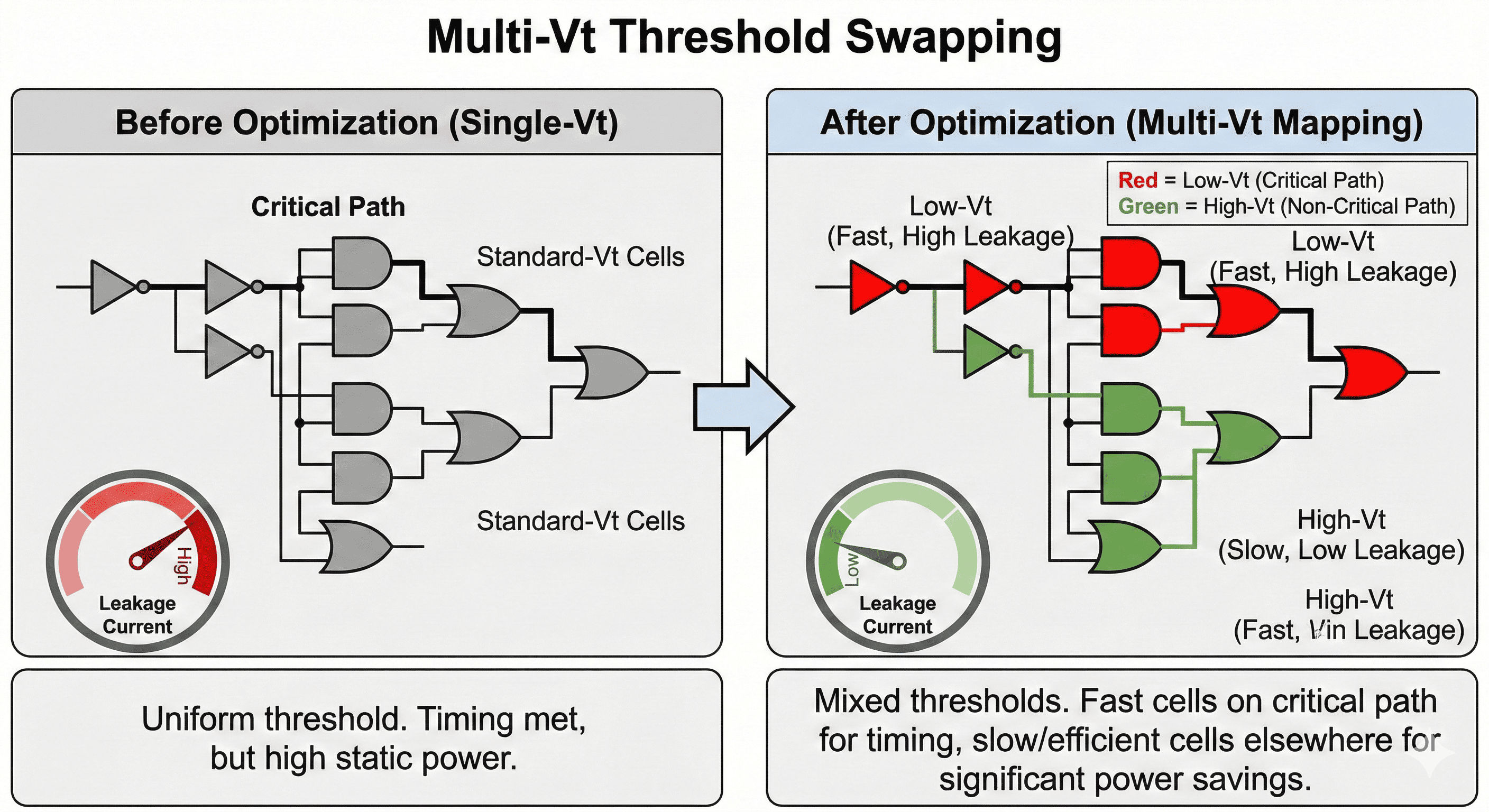
The mapping split shown here assigns threshold-voltage flavors according to path criticality and available slack. Fast but leakier cells are retained on tight timing cones, while relaxed cones are remapped to higher-Vt variants to suppress standby leakage. This targeted assignment preserves frequency goals while reducing static power without requiring architectural RTL changes.
6.2 Clock Gating Optimizations
The clock network toggles twice every cycle (rising and falling edge), consuming up to 40% of a chip's total dynamic power. Clock gating disables the clock signal to registers when their data is not actively changing.
ICG insertion behavior: Clock pulses are allowed only when enable logic indicates state updates are required, which suppresses wasteful toggling.
- Standard Clock Distribution: A standard 8-bit Register Bank continuously receives an active CLK signal. Even if the incoming data D[7:0] remains static, the internal clock tree of the register continuously toggles, hemorrhaging High Dynamic Power waste.
- Optimized with ICG: An Integrated Clock Gating (ICG) cell is physically inserted upstream of the register bank. The original CLK and an Enable control logic signal feed into the ICG, outputting a Gated Clock (GCLK). When the Enable signal drops low, GCLK is held perfectly steady, preventing the downstream register from toggling and saving massive amounts of power.
- Glitch-Free Internal Architecture: To prevent catastrophic false clock triggers (glitches), the standard ICG cell is architected using a negative-level-sensitive latch driving an AND gate. The incoming CLK drives the latch (inverted) and one leg of the AND gate, while the Enable (EN) signal controls the latch input. This internal latch ensures that the Enable signal is securely captured and only passed to the AND gate when the global clock is low, fundamentally preventing the EN signal from transitioning during a high clock phase and causing a clipped clock pulse (glitch). Multilevel Clock Gate Expansion and Collapsing: If multiple register banks share the same overarching enable signal, the synthesis tool performs multilevel expansion. It inserts a primary "parent" clock gate that disables the clock for an entire hierarchical block, feeding secondary "child" clock gates. Conversely, if activity profiling (via SAIF) shows that a parent clock gate is always enabled (toggle rate of 0), the tool collapses the hierarchy to remove the redundant gating cell, saving area and reducing clock insertion delay.
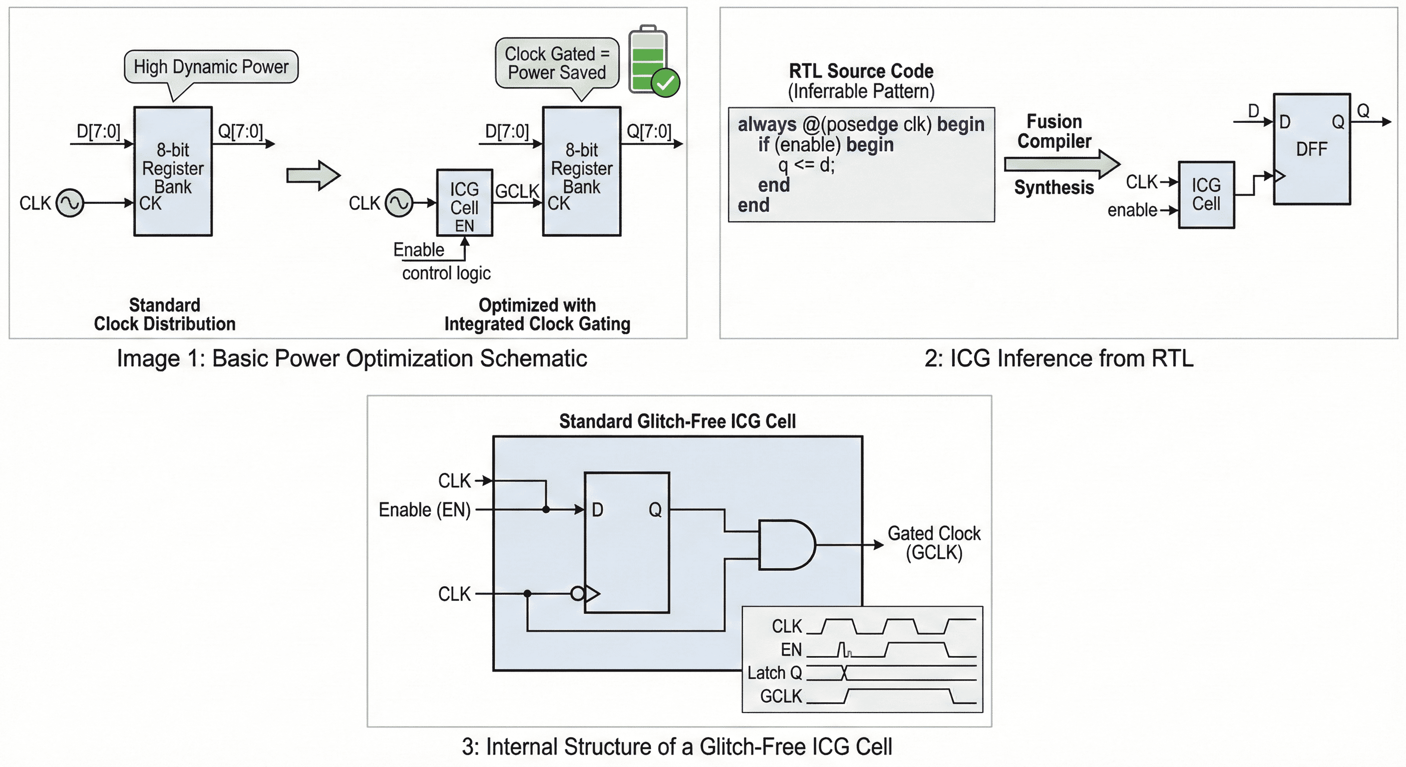
This structure gates switching at the clock entry point of a register cluster, which suppresses unnecessary toggling before it propagates through sequential elements. The latch-based control path guarantees glitch-safe enable sampling so clipped pulses are avoided. Because it disables high-capacitance clock activity directly, the savings are typically larger than data-path-only power tweaks.
6.3 Smart Registers: Self-Gating
Standard clock gating relies on explicit enable conditions written into the RTL by the designer. However, many registers receive new data every cycle, but the actual value of that data hasn't changed. Self-Gating automatically detects this scenario. The synthesis tool inserts an XOR comparator gate across the D (input) and Q (output) pins of a register. If the XOR gate determines that , the data is unchanged. The XOR output triggers an ICG cell to block the clock pulse for that specific cycle. While this adds area (the XOR gate and the ICG), if the SAIF file indicates high temporal redundancy on a wide bus, the dynamic power saved by preventing the clock pulse vastly outweighs the power consumed by the comparator logic.

The generated topology compares incoming data and stored state each cycle so the local clock is admitted only when a state update is required. When D equals Q, the enable remains inactive and the register skips redundant clock switching while function remains unchanged. This mechanism is most beneficial on wide buses with repeated values, where avoided toggles accumulate into meaningful dynamic-power reduction.
6.4 IR-Drop Mitigation
During the postroute optimization stage, regions with high densities of simultaneously switching cells suffer from severe dynamic voltage drop (IR Drop). This starvation of voltage increases cell delay unpredictably and can induce logic failures. By integrating advanced dynamic voltage drop (IR Drop) analysis natively, the synthesis tool identifies these hotspots. The engine performs Dynamic Power Shaping , actively spreading high-toggle cells apart or downsizing them to disperse the power density, successfully mitigating the IR drop while maintaining strict setup and hold timing closure.

This placement-aware diagram shows how concentrated high-toggle cells can produce localized current spikes and voltage droop on the power grid. The optimization disperses or reshapes switching demand so peak current density is reduced in hotspot windows. Lower droop improves timing stability and noise robustness, especially during simultaneous switching bursts that would otherwise destabilize critical paths.
7. Boolean Optimization
The technology-independent logic optimization stage relies on complex algorithms to restructure Boolean equations. While modern EDA tools abstract the underlying mathematics from the user through simple high-effort compilation commands, understanding these algorithms is crucial for advanced VLSI engineering.
7.1 Two-Level Logic Minimization
Two-level logic aims to reduce any Boolean function to a flattened Sum-of-Products (SOP) or Product-of-Sums (POS). The goal is to find an equivalent representation that uses the mathematical minimum number of product terms (implicants) and literals.
The Quine-McCluskey (QM) Algorithm (Exact Method) The QM algorithm is a deterministic tabular method guaranteed to find the exact global minimum SOP form, completely bypassing manual-map limitations and the error-prone nature of Karnaugh maps. 1. Prime Implicant Generation: The algorithm groups minterms by the number of '1's in their binary representation. It iteratively compares adjacent groups, applying the fundamental Boolean identity to merge terms that differ by exactly one bit. The surviving, un-mergeable terms form the exhaustive list of prime implicants . 2. Prime Implicant Table: A matrix is constructed with prime implicants as rows and original minterms as columns. The algorithm selects essential prime implicants (those that solely cover a specific minterm). It then uses row/column dominance heuristics or Petrick's method to resolve the remaining cyclic covering problem.
Limitation: The QM method exhibits exponential computational complexity. For functions exceeding roughly 15 variables, generating every prime implicant becomes computationally intractable, rendering it unsuitable for large-scale industrial VLSI design.
The Espresso Algorithm (Heuristic Method) To resolve the exponential scaling problem of QM, the Espresso heuristic logic minimizer was developed. Rather than exhaustively generating all prime implicants, Espresso operates iteratively on a localized initial cover of the function, providing near-optimal results in a fraction of the time. It loops through three core operations until the literal count stabilizes: 1. EXPAND: Greedily removes literals to expand each implicant as much as possible, turning them into prime implicants without intersecting the function's OFF-set (the matrix space where the output must be 0). 2. IRREDUNDANT COVER: Analyzes the expanded cover to identify and prune mathematically redundant implicants, extracting a minimal essential cover. 3. REDUCE: Re-adds literals to shrink the implicants as much as possible while maintaining functional coverage. This counter-intuitive step intentionally shifts the algorithm out of local mathematical minimums, creating "space" for the next EXPAND cycle to find an entirely different, potentially more optimal covering.
7.2 Multi-Level Logic Optimization
While two-level SOP logic is incredibly fast (maximum two gate delays), it requires massive fan-in gates (e.g., a 100-input OR gate) which are physically impossible or highly inefficient to manufacture in CMOS technology. Real VLSI designs use Multi-Level Logic. The circuit is modeled as a Directed Acyclic Graph (DAG), where nodes are local logic functions and edges represent the dependencies. Optimization relies on technology-independent structural transformations:
- Factoring: Extracting common variables to drastically reduce literal counts.
- Mechanism: The expression requires 8 literals, 4 AND gates, and a 4-input OR gate. Factoring reduces this to , requiring only 4 literals, 2 OR gates, and 1 AND gate.
- Decomposition: Breaking complex single nodes into networks of simpler nodes to respect the strict standard cell fan-in limits dictated by the technology library.
- Substitution: Reusing existing logic nodes to simplify others, maximizing logic sharing. If the node already exists in the DAG, the function is substituted and simplified to .
- Elimination (Collapsing): The inverse of substitution. If an intermediate node's delay penalty is too high (causing a timing violation), it is mathematically collapsed back into its fanout nodes to flatten the logic depth at the cost of duplicating logic area. Synthesis tools leverage both Algebraic methods (which treat logic like standard polynomial algebra for extreme speed, ignoring identities like ) and Boolean methods (which utilize full Boolean identities and "don't care" conditions for exact optimization). Modern tools apply fast algebraic factoring first to structure the DAG, followed by localized Boolean optimization on the most critical control paths to squeeze out the final margins of area and delay.
The simplification flow illustrates how factoring, decomposition, and selective collapsing are combined to build realizable multi-level logic. Complex equations are restructured into smaller shared nodes that respect library fan-in limits while preserving optimization freedom. This balance is critical in silicon implementation because it controls depth, gate count, and electrical load simultaneously instead of optimizing only one metric.
8. Optimization Summary
Logic synthesis represents a monumental triumph of computational mathematics applied to physical engineering. By mastering the deep interactions between Boolean algorithms, tool constraints, and physical reality, engineers can confidently drive complex VLSI designs from abstract behavioral code to sign-off and successful silicon realization. Below is a categorized summary of the primary optimization methodologies utilized to balance the triad of VLSI constraints: Power, Area, and Timing.
Table 1: Power Optimization Methods
| Method | Description |
|---|---|
| Clock Gating (ICG) | Inserts integrated clock-gating cells to disable clock toggling to idle registers, eliminating massive dynamic power waste. |
| Multi-Vt Swapping | Swaps Standard-Vt cells on non-critical paths for slow, highly efficient High-Vt variants to drastically reduce static leakage. |
| Self-Gating | Inserts comparator (XOR) logic to block clock pulses when incoming cycle data matches the existing register state. |
| Multibit Banking | Groups single-bit registers to share clock/reset drivers, greatly reducing the total clock tree capacitance and switching power. |
| Dynamic Power Shaping | Analyzes switching profiles to physically disperse high-toggle cells during placement, mitigating dynamic IR drop hotspots. |
| Register Merging | Eliminates logically redundant registers that receive identical inputs and controls, reducing the total number of toggling flip-flops. |
Table 2: Area Optimization Methods
| Method | Description |
|---|---|
| Boundary Optimization | Propagates constants and pushes phase inverters across hierarchical module boundaries to eliminate redundant gates. |
| Boolean Minimization | Employs heuristic algorithms (like Espresso) to algebraically reduce the literal count and necessary gate implementation. |
| Area Recovery Downsizing | Actively downsizes high-drive-strength standard cells on timing paths with excess positive slack to reclaim physical area. |
| Factoring & Substitution | Restructures complex multi-level logic into shared, reusable sub-expressions to minimize total gate count. |
| Multibit Banking | Merges individual flip-flops into shared macro cells, eliminating the redundant control-logic transistors found in single bits. |
| Register Merging | Identifies and merges multiple equivalent registers into a single register, directly removing redundant logic gates from the netlist. |
Table 3: Timing Optimization Methods
| Method | Description |
|---|---|
| Datapath Extraction | Replaces slow, cascaded ripple-carry logic with high-speed, parallel architectures such as Carry-Save Adder (CSA) trees. |
| Concurrent Clock and Data (CCD) | Adjusts individual clock latencies (useful skew) to borrow time from fast paths and donate it to paths failing setup time. |
| Register Replication | Duplicates heavily loaded registers to split the fanout, reducing capacitive delay and accelerating the signal transition. |
| Logic Flattening | Collapses deep multi-level logic cones into wider, shallower logical structures to reduce the maximum gate delay depth. |
| Gate Sizing & Buffering | Upsizes critical cells to higher drive strengths or inserts buffer repeaters to push signals faster across highly resistive wires. |