CMOS Fundamentals
From semiconductor physics to MOSFET behavior, one clear step at a time.
The Foundation of Solid-State Electronics
Modern VLSI may look like a world of EDA tools, timing reports, and placement constraints, but it still starts with a simpler question: when does silicon allow charge to move, and when does it block it? That answer comes from semiconductor physics. Once you understand carrier motion, energy bands, and PN junction behavior, the rest of CMOS stops feeling mysterious and starts looking like a controlled extension of those basic ideas.
1.1 Semiconductor Physics and the Flow of Electricity
The electrical behavior of a solid depends on how its atoms are arranged and on which energy states its electrons are allowed to occupy. In a single atom, those states are discrete. In a crystal, where a huge number of atoms sit in a regular lattice, the same states spread out into bands. That shift from isolated energy levels to energy bands is the starting point for understanding why some materials conduct easily, some barely conduct at all, and silicon sits in the useful middle.
The doping story is easiest to follow with Figure 1 and Figure 2. Figure 1 compares intrinsic, n-type, and p-type silicon in one view, while Figure 2 shows the same shift using the Fermi level. Together, they make the ideas of majority carriers and energy-band shift much easier to see.
.webp)
.webp)
- Energy Bands and the Band Gap: In a semiconductor like silicon (Si), two primary energy bands dictate its electrical behavior: the valence band (Ev) and the conduction band (Ec). The valence band represents the energy levels of the outermost electrons that are bound to their respective atoms. The conduction band represents the energy levels of electrons that have broken free from their atomic bonds and are able to move throughout the crystal, thereby conducting electricity. These two bands are separated by a forbidden energy range known as the band gap (Eg). For silicon at room temperature, the band gap is approximately 1.12 eV. For an electron to conduct electricity, it must gain enough energy to jump from the valence band, across the band gap, and into the conduction band. When this occurs, it leaves behind a vacancy in the valence band, known as a hole, which can be considered a mobile positive charge carrier.
- Intrinsic and Extrinsic Semiconductors: A pure semiconductor crystal is called an intrinsic semiconductor. At absolute zero temperature, its valence band is completely full and its conduction band is empty, making it a perfect insulator. At room temperature, thermal energy is sufficient to excite a small number of electrons into the conduction band, creating an equal number of electrons and holes. The intrinsic carrier concentration in silicon, denoted ni, is approximately 1.45 × 1010 cm-3 at 300 K, which is too low for most practical applications. To dramatically increase the conductivity, semiconductors are intentionally doped with impurity atoms, a process that creates extrinsic semiconductors.
- N-type Doping: Introducing pentavalent atoms (e.g., Phosphorus, Arsenic), which have five valence electrons, into the silicon lattice creates an excess of free electrons. These impurity atoms are called donors. The energy level of these donor electrons is very close to the conduction band, so they are easily excited into it, becoming mobile charge carriers. In an n-type semiconductor, electrons are the majority carriers and holes are the minority carriers.
- P-type Doping: Introducing trivalent atoms (e.g., Boron), which have three valence electrons, creates a deficiency of one electron, or a hole. These impurity atoms are called acceptors. The energy level of these acceptor states is very close to the valence band, making it easy for a valence electron to move into this state, effectively creating a mobile hole. In a p-type semiconductor, holes are the majority carriers and electrons are the minority carriers.
- The Fermi Level: The Fermi level (EF) is a conceptual energy level that represents the statistical probability of an energy state being occupied by an electron. In an intrinsic semiconductor, EF lies near the middle of the band gap. Doping shifts the Fermi level: in an n-type material, EF moves closer to the conduction band, while in a p-type material, it moves closer to the valence band. This shift is a direct consequence of the altered carrier concentrations and is a key concept for understanding the behavior of semiconductor junctions.
- Carrier Transport Mechanisms: The movement of charge carriers (electrons and holes) constitutes the flow of electricity. There are two primary mechanisms for this transport:
- Drift: The movement of charge carriers under the influence of an applied electric field (E). Electrons drift in the direction opposite to the field, while holes drift in the same direction. The resulting drift current density is proportional to the electric field and the carrier concentration.
- Diffusion: The movement of charge carriers from a region of high concentration to a region of low concentration. This movement is a natural statistical process driven by the concentration gradient and does not require an electric field. The resulting diffusion current is proportional to the gradient of the carrier concentration.
The interplay between drift and diffusion is the central principle governing the operation of the PN junction.
1.2 The PN Junction Diode in Equilibrium
The PN junction is the first structure where semiconductor physics turns into a usable device. Put p-type material next to n-type material and the carriers immediately react to the concentration difference. That single interface becomes the basis for diodes, bipolar devices, and the source/drain junctions that appear inside MOSFETs.
- Formation of the Depletion Region: Immediately upon formation of the junction, a steep concentration gradient exists for both majority carriers. Holes from the p-side diffuse into the n-side, and electrons from the n-side diffuse into the p-side. As these carriers cross the junction, they leave behind the fixed, ionized impurity atoms: negatively charged acceptor ions (NA-) on the p-side and positively charged donor ions (ND+) on the n-side. This process creates a region near the metallurgical junction that is depleted of mobile charge carriers, known as the depletion region or space charge region.
- Built-in Potential and Energy Bands: The layer of fixed positive and negative charges in the depletion region establishes an internal electric field that points from the n-side to the p-side. This field opposes the further diffusion of majority carriers. The diffusion process continues until the force of the electric field on the carriers perfectly balances the tendency for diffusion. At this point, the system is in thermal equilibrium, and there is no net flow of current across the junction.
The total potential difference across the depletion region in equilibrium is called the built-in potential, φ0, given by the equation: φ0 = (kT/q) * ln(NAND / ni2)
where k is Boltzmann's constant, T is the absolute temperature, and q is the elementary charge.
The energy band diagram provides the clearest visualization of this equilibrium state. For the system to be in equilibrium, the Fermi level (EF) must be constant throughout the entire structure. To achieve this alignment, the energy bands of the p-type and n-type regions must shift relative to each other. The bands on the p-side are higher in energy than the bands on the n-side, resulting in a bending of the conduction and valence bands across the depletion region. This band bending creates a potential energy barrier of height qφ0 that majority carriers must overcome to diffuse across the junction.
.webp)
Equilibrium does not mean nothing is happening. It means two opposite processes cancel each other exactly. Diffusion pushes majority carriers across the junction, while the built-in electric field pulls minority carriers the other way by drift. The measured current is zero only because those two internal currents are equal. That idea matters, because biasing the junction simply breaks this balance. Figure 3 shows that balance in carrier-flow language rather than band language.
.webp)
1.3 The Junction Under Bias
Once an external voltage is applied, the junction leaves equilibrium. The job of the applied bias is simple: it either lowers the barrier so carriers can cross more easily, or raises it so current is strongly suppressed.
- Forward Bias: When a positive voltage is applied to the p-side with respect to the n-side, the external field opposes the internal built-in field. This reduces the potential energy barrier across the depletion region. With a lower barrier, the diffusion of majority carriers across the junction increases exponentially. The diffusion current becomes much larger than the small, opposing drift current, resulting in a significant net current flow from the p-side to the n-side. The energy band diagram for forward bias shows the Fermi levels being separated by the applied voltage, which effectively lowers the height of the potential barrier.
- Reverse Bias: When a negative voltage is applied to the p-side with respect to the n-side, the external field aids the internal built-in field. This increases the height of the potential energy barrier, further suppressing the diffusion of majority carriers. The diffusion current becomes negligible. The drift current, which depends on the concentration of minority carriers, remains largely unaffected and constitutes a very small reverse saturation current. This current flows from the n-side to the p-side and is nearly independent of the applied reverse voltage. The energy band diagram shows the Fermi levels separating further apart, increasing the barrier height.
This one-way current behavior is called rectification. In practice, it is what makes the diode useful: forward bias gives you strong conduction, while reverse bias gives you isolation except for a small leakage current.
Figure 5 is worth reading next to the text because it turns the idea into one simple visual rule: forward bias lowers the barrier and encourages majority-carrier transport, while reverse bias widens the barrier and leaves only a small leakage path.
.webp)
The Metal-Oxide-Semiconductor (MOS) System
The PN junction gives us the basic electrostatics, but the transistor that drives digital VLSI is the MOSFET. Its power comes from field control. Instead of forcing carriers across a junction, the gate reshapes the charge distribution at the silicon surface and decides whether a conducting path exists at all.
2.1 MOSFET Structure
The MOSFET turns the MOS idea into a real switching device by adding two heavily doped terminals, source and drain, on either side of the gate. Once those terminals exist, the inversion layer is no longer just a surface-charge effect. It becomes the path through which current can move.
- nMOS Structure: An n-channel MOSFET (nMOS) uses a p-type body with two n+ regions for source and drain. The gate sits above a thin SiO2 layer, and the silicon directly under the gate becomes the channel region. When the gate bias is large enough, an electron channel forms and connects source to drain. Figure 6 is the cleanest way to see where the source, drain, gate, oxide, and body actually sit in that stack.
.webp)
- pMOS Structure: A p-channel MOSFET (pMOS) is the complementary device. It uses an n-type body or n-well with p+ source and drain regions, and it conducts by forming a hole channel under the gate. Figure 7 keeps the geometry familiar while flipping the carrier type and bias direction.
.webp)
- Why CMOS Uses Both: CMOS logic places nMOS and pMOS devices together so one side pulls a node down while the other pulls it up. That complementary action is the reason CMOS gives strong logic levels with low static power.
2.2 The MOS Capacitor
The MOS capacitor is the cleanest way to see how the gate controls silicon. It is just a gate electrode, a thin oxide, and a semiconductor body. But that simple stack is enough to show the full story. A gate voltage builds an electric field across the oxide, and that field changes the carrier concentration right at the silicon surface. Before any external bias is applied, the structure sits in thermal equilibrium, shown in Figure 8.
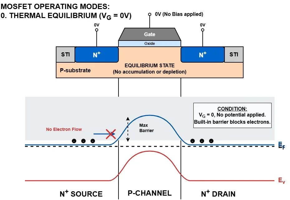
From that starting point, the gate bias drives the surface through three recognizable regimes.
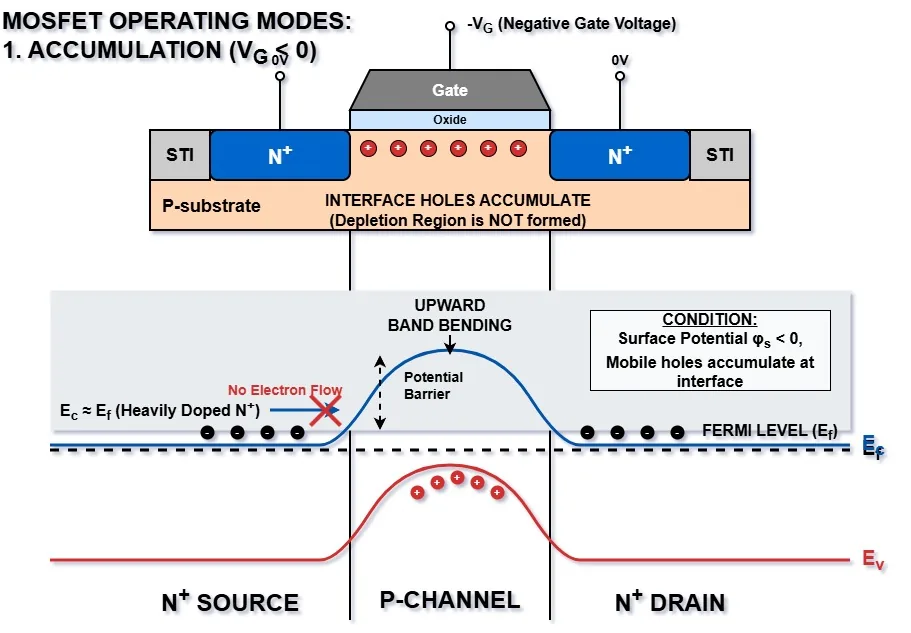
- Accumulation (VG < 0): A negative voltage on the gate attracts the majority carriers (holes) from the p-type substrate to the silicon-oxide interface. This results in a higher concentration of holes at the surface than in the bulk, a condition known as accumulation. The energy bands at the surface bend upwards, indicating an increase in potential energy for electrons and a decrease for holes, which draws the valence band edge closer to the Fermi level. Figure 9 shows that crowding of holes right at the interface.
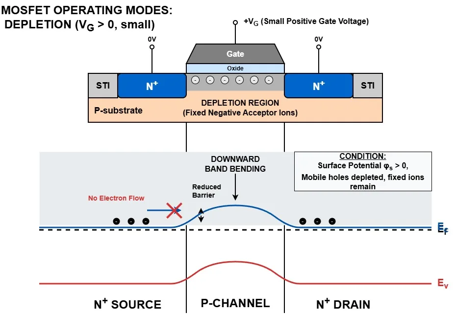
- Depletion (VG > 0, small): A small positive voltage on the gate repels the mobile majority carriers (holes) from the interface, pushing them deeper into the substrate. This leaves behind a region near the surface that is depleted of mobile carriers and contains only fixed, negatively charged acceptor ions (NA-). This is the depletion region. The energy bands at the surface bend downwards, indicating that the surface potential has increased. Figure 10 captures that transition clearly: mobile holes retreat, but the fixed charge remains.
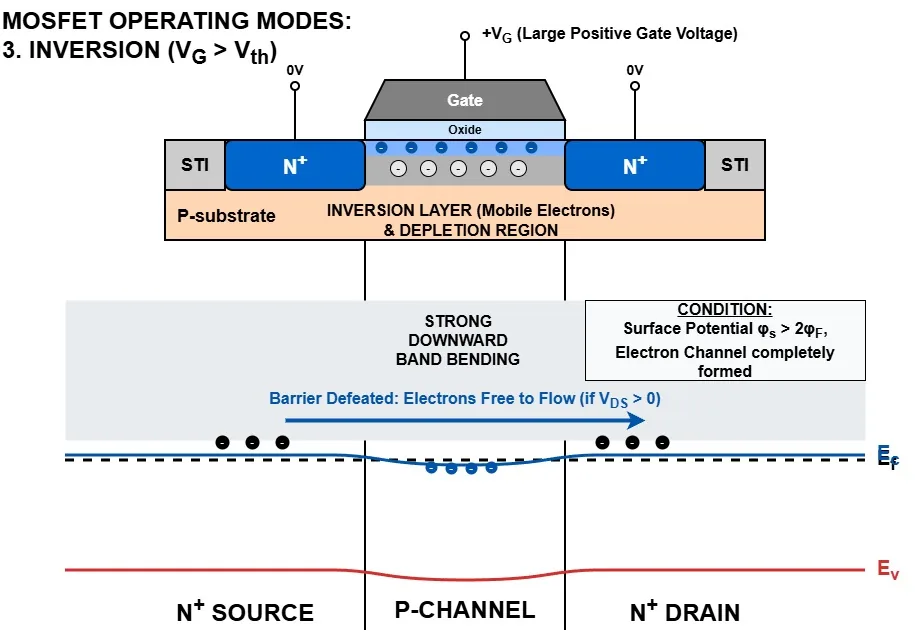
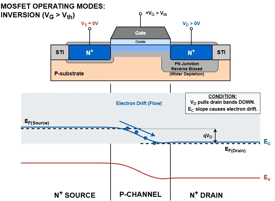
- Inversion (VG > Vth): As the positive gate voltage is increased further, the downward bending of the energy bands becomes more pronounced. Eventually, the gate voltage becomes strong enough to attract minority carriers (electrons) from the bulk to the surface. When the concentration of these electrons at the surface becomes greater than the concentration of holes in the bulk, the surface is said to be inverted. This thin layer of mobile electrons at the interface forms a conducting n-channel. The gate voltage at which strong inversion occurs is known as the threshold voltage (Vth). In the energy band diagram, strong inversion corresponds to the point where the intrinsic Fermi level at the surface (Ei) drops below the bulk Fermi level (EF), and the surface potential becomes equal in magnitude but opposite in sign to the bulk Fermi potential (φS = -2φF). Figure 11 is the key transition, because this is where the surface stops behaving like depleted p-type silicon and starts behaving like a usable channel.
2.3 MOSFET Operation and I-V Characteristics
Once the device structure and MOS electrostatics are clear, the operation becomes easier to read. The gate-to-source voltage (VGS) decides whether a channel exists, and the drain-to-source voltage (VDS) decides how strongly that channel is used. The I-V curves simply translate those two voltages into current.
- Cut-off Region (VGS < Vth): No inversion layer is formed, and the path between source and drain behaves like two back-to-back PN junctions. The transistor is OFF, and the drain current is ideally zero (ID = 0).
- Linear (or Triode) Region (VGS > Vth and VDS < VGS - Vth): In this region, a continuous conductive channel exists from source to drain. For a small VDS, the drain current is approximately proportional to VDS, meaning the device behaves like a voltage-controlled resistor. As VDS increases, the voltage drop along the channel reduces the effective gate-to-channel voltage near the drain, causing the channel to become less conductive there. This results in a sub-linear increase of ID with VDS. The current is given by:
Here, μn is the electron mobility, Cox is the gate oxide capacitance per unit area, and W and L are the channel width and length, respectively.ID = μnCox(W/L) * [(VGS - Vth)VDS - VDS2/2] - Saturation Region (VGS > Vth and VDS ≥ VGS - Vth): When VDS reaches the value VGS - Vth, the effective gate-to-channel voltage at the drain end becomes zero. At this point, the inversion channel is said to be "pinched off" at the drain. For any further increase in VDS, the pinch-off point moves slightly toward the source, and the voltage at this point remains fixed at VGS - Vth. Electrons arriving at the pinch-off point are then swept across the drain's depletion region by the high electric field. To a first-order approximation, the drain current becomes independent of VDS and is controlled only by VGS. The device now behaves like a voltage-controlled current source. The saturation current is given by:
ID = (1/2) * μnCox(W/L) * (VGS - Vth)2
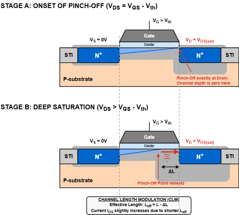
This mix of behaviors is exactly why the MOSFET is so useful. The same device can look like an open switch, a controlled resistor, or a current source depending on the operating point. Figure 12 gives the physical picture of the channel under positive VDS, while Figure 13 shows the pinch-off condition that defines deep saturation. In a CMOS inverter, one device may be charging or discharging the output in saturation while the other behaves more like a resistive path. Good digital switching comes from that interaction, not from a single simplified device mode.
The Threshold Voltage and Second-Order Effects
The threshold voltage (Vth) is the line between "channel not formed well enough" and "device conducts strongly enough to use." In first-pass analysis we often treat it as a fixed number. Real transistors do not give us that luxury. Bias conditions, geometry, and short-channel physics all move Vth around, and those shifts directly affect speed, leakage, and noise margins.
3.1 Defining the Threshold Voltage (Vth)
Threshold voltage is the minimum gate-to-source voltage needed to form strong inversion under the gate. It is not set by one knob; it comes from several physical contributions in the MOS stack:
- Work Function Difference (ΦGC): The difference between the work function of the gate material (e.g., polysilicon) and the semiconductor substrate. This term accounts for the built-in potential of the MOS system.
- Surface Inversion Component (−2φF): The portion of the gate voltage needed to bend the energy bands sufficiently to achieve strong inversion at the surface. φF is the bulk Fermi potential of the substrate.
- Depletion Charge Component (−QB0/Cox): The voltage required to offset the charge of the fixed ions in the depletion region that forms under the gate before inversion occurs.
- Fixed Oxide Charge Component (−Qox/Cox): The voltage needed to compensate for fixed positive charges that are trapped at the silicon-oxide interface during fabrication.
Combining these terms gives the expression for the zero-bias threshold voltage, VT0: VT0 = ΦGC − 2φF − QB0/Cox − Qox/Cox
3.2 The Body Effect (Substrate Bias Effect)
In real circuits, the source terminal is often not sitting at the same potential as the body. That is common in stacked logic, transmission structures, and many internal nodes. Once VSB is non-zero, the channel no longer forms at the same gate voltage as before.
- Mechanism: A positive VSB (for an nMOS device) acts as a reverse bias on the source-substrate junction. This widens the depletion region beneath the gate, increasing the total amount of fixed negative charge (QB) that the gate voltage must overcome to form the channel.
- Impact: To compensate for this larger depletion charge, a higher gate voltage is required to achieve inversion. Consequently, the threshold voltage increases. This phenomenon is known as the body effect or substrate bias effect. The change in Vth is described by the following equation:
where γ is the body-effect coefficient, which depends on the substrate doping and oxide thickness.VT = VT0 + γ(√(|−2φF + VSB|) − √(|2φF|))
The body effect shows up immediately in real standard cells. In a two-input NAND gate, the pull-down network uses two nMOS transistors in series. When both inputs are high, the source of the upper device rises above ground, which means VSB is no longer zero. Its threshold voltage increases, the device becomes weaker, and designers often compensate by increasing its W/L ratio. That fix improves current, but it also costs area and adds input capacitance.
3.3 Channel Length Modulation and Velocity Saturation
As the channel gets shorter, the clean long-channel picture starts to bend. Effects that used to look like minor corrections begin to shape the current directly. That is why modern device behavior has to be read with geometry in mind, not just with the basic square-law equations.
- Channel Length Modulation (CLM): In the saturation region, the drain current is ideally independent of VDS. In reality, as VDS increases beyond the saturation point (VDSAT), the depletion region around the drain expands and the channel pinch-off point moves slightly toward the source. This reduces the effective channel length (Leff). Since drain current is inversely proportional to channel length, this effect causes the saturation current to increase slightly with VDS. This gives the transistor a finite output resistance and is modeled by adding a corrective term to the saturation current equation:
where λ is the channel length modulation parameter.ID,sat = ID,sat,ideal ⋅ (1 + λVDS) - Velocity Saturation: In long-channel devices, carrier velocity is proportional to the electric field. In short-channel devices, the lateral electric field along the channel can be very high (>104 V/cm). At such high fields, the velocity of charge carriers no longer increases linearly with the field and approaches a saturation velocity (vsat). This means the current delivered by the transistor stops increasing quadratically with VGS in saturation and becomes approximately linear. This effect limits the maximum current a transistor can provide, reducing its drive strength compared to what long-channel models would predict.
The practical takeaway is simple: transistor parameters move with bias and geometry. In modern VLSI, managing those shifts through modeling, cell design, and signoff analysis is part of the job, not a refinement added at the end.
3.4 Drain-Induced Barrier Lowering (DIBL)
Drain-Induced Barrier Lowering shows up when the drain gets strong enough to interfere with a job that should mostly belong to the gate. In a long-channel device, the source-side barrier is controlled mainly by gate electrostatics. In a short-channel device, a large drain voltage reaches back into the channel and pulls that barrier down.
That change matters because the transistor can begin to conduct more easily even though VGS has not increased. In plain terms, the apparent threshold voltage falls as VDS rises. The off-state gets leakier, subthreshold current increases, and bias conditions that once looked safe start to move. Figure 14 gives the quick intuition, and Figure 15 shows the same idea with a more detailed electrostatic picture.
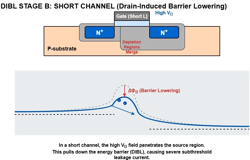
Figure 14 gives the quick picture: a stronger drain does not just wait at the end of the channel. It reaches toward the source and makes it easier for carriers to enter.
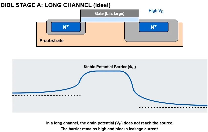
Figure 15 adds the deeper message: DIBL is not just a leakage keyword. It is a sign that the device electrostatics are being shared between terminals in a way that hurts threshold stability.
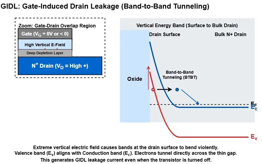
3.5 Gate-Induced Drain Leakage (GIDL)
GIDL is a different leakage path from ordinary subthreshold current. It does not require a fully formed channel between source and drain. Instead, it appears near the drain-side edge of the gate when the local electric field becomes extremely strong.
Under that field, band-to-band tunneling can generate carriers near the gate-drain overlap region. That means leakage can appear even when the transistor is supposed to be off. The important distinction is that the current is born near the drain edge, not simply because the entire channel barrier has dropped. Figure 16 and Figure 17 make that local high-field picture much easier to see.
.webp)
In scaled technologies, GIDL matters in high-field corners, IO devices, and bias conditions where the gate and drain create a harsh local field. That is why device engineers pay attention to overlap design, junction shaping, and oxide field management instead of treating leakage as a single-number problem.
The CMOS Inverter: Static and Dynamic Behavior
The CMOS inverter is the first complete digital building block worth mastering. It looks simple, but it contains the same ideas that appear again in larger logic: complementary pull-up and pull-down action, a well-defined transfer curve, useful noise margins, and delay set by current charging or discharging capacitance. The circuit uses one nMOS and one pMOS transistor with their gates tied together and their drains tied together to implement the NOT function cleanly and efficiently.
4.1 The Ideal Inverter and Performance Metrics
An ideal inverter would switch instantly and cleanly. Its Voltage Transfer Characteristic (VTC), a plot of Vout versus Vin, would have a few obvious features:
- An output voltage swing from rail to rail (0 to VDD).
- An infinitely high gain in the transition region.
- A switching threshold voltage (Vth) precisely at VDD/2.
- Perfectly defined logic levels, where any input below Vth produces a high output, and any input above Vth produces a low output.
Real inverters do not switch that sharply. To describe how close a practical design gets, we define a set of voltage points and robustness metrics:
- VOH (Output High Voltage): The maximum output voltage when the input is low. For a CMOS inverter, VOH = VDD.
- VOL (Output Low Voltage): The minimum output voltage when the input is high. For a CMOS inverter, VOL = 0.
- VIL (Input Low Voltage): The maximum input voltage that is reliably interpreted as a logic '0'. It is defined as the point on the VTC where the slope, dVout/dVin, equals -1.
- VIH (Input High Voltage): The minimum input voltage that is reliably interpreted as a logic '1'. It is also defined at the point where the slope of the VTC is -1.
- Noise Margins: These metrics quantify the circuit's ability to tolerate noise on its input. A larger noise margin indicates a more robust design.
- Low Noise Margin (NML): NML = VIL − VOL
- High Noise Margin (NMH): NMH = VOH − VIH
4.2 The CMOS Inverter: DC Analysis
The DC analysis comes from matching the pull-down current of the nMOS and the pull-up current of the pMOS as the input sweeps from 0 to VDD. That current balance breaks the VTC into five operating regions, depending on whether each device is in cut-off, linear, or saturation.
- Region A (Vin < VTn): The nMOS is in cut-off, the pMOS is in the linear region. No current flows, and Vout = VOH = VDD.
- Region B (VTn ≤ Vin < Vth): The nMOS enters saturation, while the pMOS remains in the linear region. Vout begins to drop as Vin increases. The point VIL lies within this region.
- Region C (Vin = Vth): Both transistors are in saturation. This is the transition region where the VTC is steepest. The switching threshold voltage (Vth) is the point where Vin = Vout. By equating the saturation current equations for both transistors, Vth can be derived:
where kn = μnCox(W/L)n and kp = μpCox(W/L)p.Vth = (VT0,n + √(kp/kn)(VDD + VT0,p)) / (1 + √(kp/kn)) - Region D (Vth < Vin ≤ VDD + VTp): The nMOS transitions to the linear region, while the pMOS remains in saturation. Vout continues to fall. The point VIH lies within this region.
- Region E (Vin > VDD + VTp): The pMOS is in cut-off, the nMOS is in the linear region. No current flows, and Vout = VOL = 0.
4.3 Inverter Sizing and Performance
The shape of the VTC, and therefore the switching point and noise margins, depends strongly on the ratio between nMOS and pMOS drive strength. Designers often call this the beta ratio (βn/βp) or the transconductance ratio (kR = kn/kp).
A symmetric inverter is designed to have Vth = VDD/2, which generally maximizes the noise margins and provides equal rise and fall times. To achieve this, the pull-up (pMOS) and pull-down (nMOS) networks must have equal drive strengths. This requires setting the transconductance ratio such that it compensates for the mobility difference, typically meaning (W/L)p ≈ (2 to 3) × (W/L)n. Adjusting this ratio shifts the VTC: increasing the nMOS strength (higher kR) shifts the VTC to the left, while increasing the pMOS strength (lower kR) shifts it to the right.
4.4 Inverter Switching Characteristics
Dynamic behavior answers a different question: once the input changes, how fast does the output move? The propagation delay is mainly the time required to charge or discharge the total load capacitance (Cload) connected to the output node.
- Propagation Delays (τpHL and τpLH):
- τpHL (high-to-low): The delay for the output to fall from 50% of VDD in response to the input rising to 50% of VDD. This transition is driven by the nMOS transistor pulling the output node to ground.
- τpLH (low-to-high): The delay for the output to rise, driven by the pMOS transistor charging the output node to VDD.
The key relationship is I = C(dV/dt). A stronger transistor can move more current and change the node voltage faster. But that same larger device adds gate and diffusion capacitance, which loads the previous stage. So sizing is never free. You gain drive strength locally and pay for it somewhere else in the path.
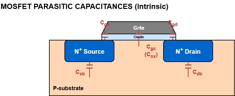
Delay is never set by an ideal load alone. Figure 18 marks the extra capacitances that sit around a real MOSFET, including overlap capacitance, junction capacitance, and gate capacitance. Every transition has to charge or discharge those hidden capacitors too.
In CMOS switching, power is usually discussed in three pieces: dynamic power from charging and discharging capacitance, short-circuit power during the brief overlap when both devices conduct, and static leakage power when the gate is nominally idle. That basic split is enough to connect inverter behavior to later power analysis.
The advantage of CMOS becomes even clearer when it is compared with older inverter styles.
Table 1: Comparison of Inverter Technologies
| Characteristic | Resistive Load nMOS | Depletion-Load nMOS | Pseudo-nMOS | Static CMOS |
|---|---|---|---|---|
| VOH | VDD | VDD | VDD | VDD |
| VOL | >0 (Ratioed) | >0 (Ratioed) | >0 (Ratioed) | 0 |
| Noise Margin Low (NML) | Poor | Fair | Poor | Excellent |
| Noise Margin High (NMH) | Good | Good | Good | Excellent |
| Static Power Dissipation | High (when output is low) | High (when output is low) | High (when output is low) | Near Zero |
| Area | Very Large (resistor) | Moderate | Small | Small |
| Complexity | Simple | Moderate | Simple | Higher |
This comparison makes the CMOS advantage easy to see. Rail-to-rail output gives large, balanced noise margins, and in either steady logic state one transistor is off, so there is no direct DC path from VDD to ground. That near-zero static power is the main reason CMOS replaced the older ratioed styles for mainstream digital design.
Combinational and Sequential Logic Design
Once the inverter is clear, larger logic gates become much easier to read. The same complementary design idea scales from a single NOT gate to NANDs, NORs, AOI/OAI structures, and the storage elements that give digital systems memory.
5.1 Static CMOS Logic Gates
Static CMOS gates use a pull-up network (PUN) made of pMOS devices and a pull-down network (PDN) made of nMOS devices. One network connects the output to VDD, the other to ground, and the two are built as logical duals.
- Design Principle: The structure of these networks directly implements Boolean logic.
- nMOS transistors in series implement an AND function in the PDN. A path to ground exists only if all series transistors are ON.
- nMOS transistors in parallel implement an OR function in the PDN. A path to ground exists if any parallel transistor is ON.
- Duality: The PUN is the logical dual of the PDN. Where the PDN has series-connected nMOS transistors, the PUN has parallel-connected pMOS transistors, and vice-versa. This ensures that for any valid input combination, either the PUN or the PDN is ON, but never both simultaneously, thus maintaining the low static power characteristic of CMOS.
- NAND and NOR Gates:
- NAND Gate: The PDN consists of nMOS transistors in series, and the PUN consists of pMOS transistors in parallel. The output is low only when all inputs are high.
- NOR Gate: The PDN consists of nMOS transistors in parallel, and the PUN consists of pMOS transistors in series. The output is low if any input is high.
- Complex Gates (AOI/OAI): CMOS technology excels at implementing complex logic functions like AND-OR-INVERT (AOI) and OR-AND-INVERT (OAI) in a single stage. For example, the function F = (A⋅B + C)' can be built with a PDN that has two series nMOS (for A and B) in parallel with a single nMOS (for C), and a corresponding dual PUN.
5.2 Logical Sizing and EDA Tools
Complex gates only work well when the transistor sizes are chosen carefully. Sizing means adjusting W/L so the gate meets delay targets without creating excessive capacitance or area.
- The Sizing Problem: The worst-case delay must be considered. For an n-input NAND gate, the worst-case pull-down path involves all n nMOS transistors in series. To match the resistance of a single nMOS in a reference inverter, each of these series transistors must be sized up by a factor of n (i.e., have a width of nW). Conversely, for an n-input NOR gate, the worst-case pull-up path has n pMOS transistors in series, requiring each to be sized up by a factor of n. This leads to a significant increase in area and input capacitance, particularly for NOR gates with many inputs.
- Impact of Sizing on Performance: Sizing up a transistor increases its drive strength (reducing its delay) but also increases its gate capacitance. This increased capacitance becomes a larger load for the preceding gate in the logic path, slowing it down. This fundamental trade-off means that optimizing a single gate in isolation is insufficient; performance must be optimized across an entire logic path.
- Role of EDA Tools: This complex, multi-variable optimization is handled by modern Electronic Design Automation (EDA) tools. During logic synthesis and physical design, these tools use sophisticated algorithms to size gates along timing-critical paths. They rely on detailed timing models for each library cell (e.g., Non-Linear Delay Model - NLDM, or Composite Current Source - CCS) to predict the impact of sizing changes. The core principle behind many of these algorithms is Logical Effort, a framework that formalizes the trade-off between a gate's inherent complexity (logical effort) and the load it must drive (electrical effort). For a path to have minimum delay, the total effort should be distributed evenly across all stages. EDA tools iteratively resize gates to balance this effort, thereby meeting timing constraints while minimizing area and power penalties.
5.3 Sequential Logic: Latches and Flip-Flops
Combinational logic reacts to the input of the moment. Sequential logic keeps state, which lets the circuit remember what happened earlier. That memory starts with bistable feedback.
- Bistable Elements: The simplest memory element is formed by cross-coupling two inverters. This circuit has two stable states (one output high and the other low, or vice-versa) and will hold its state indefinitely as long as power is supplied.
- Latches (Level-Sensitive): A latch is a memory element whose output can change whenever its clock (or enable) input is active.
- SR Latch: Formed from cross-coupled NOR or NAND gates, it has Set (S) and Reset (R) inputs to control its state.
- Clocked D-Latch: A more common variant that has a single data input (D) and a clock input (CLK). When CLK is high, the latch is transparent, meaning its output Q follows the D input. When CLK goes low, the latch stores the value of D at that instant and holds it until the next active clock phase.
- Flip-Flops (Edge-Triggered): A flip-flop is a memory element that samples its input and changes its output only at a specific instant in time, the active edge of the clock signal.
- Master-Slave D-Flip-Flop: A common implementation consists of two cascaded D-latches. The first latch (the master) is controlled by the clock signal, while the second (the slave) is controlled by the inverted clock signal. For a positive-edge-triggered flip-flop:
- When CLK is low, the master latch is transparent and samples the D input. The slave latch is closed and holds the previous value.
- On the rising edge of CLK, the master latch closes, capturing the value of D at that instant. At the same time, the slave latch becomes transparent and passes the newly captured value from the master to the final output Q.
- When CLK is high, the slave latch remains transparent, but its input from the master is stable. The master latch is closed and ignores any further changes on D.
- Master-Slave D-Flip-Flop: A common implementation consists of two cascaded D-latches. The first latch (the master) is controlled by the clock signal, while the second (the slave) is controlled by the inverted clock signal. For a positive-edge-triggered flip-flop:
VLSI MOSFET Lab
Each plot has its own local sliders, so the output, transfer, and transconductance views can be explored independently.
Graph 1: IDS vs VDS at different VGS
This is the classic output family. As VGS rises, the channel gets stronger, the current rises, and the knee shifts because saturation begins near VDS = VGS - Vth.
IDS = 0.93 mA
The highlighted curve tracks its own VGS setting, while the marker shows one operating point directly on the family.
Graph 2: IDS vs VGS at different VDS
This transfer family shows how the same device looks as the drain bias changes. A low VDS keeps the device in the linear region longer, while a higher VDS pushes the curve closer to saturation behavior.
The transfer family responds to its own drain-bias slider, so it can be explored independently from the other plots.
Graph 3: gm vs VGS at different VDS
Transconductance tells you how much extra drain current you gain from a small change in gate voltage. Showing it as a drain-bias family makes the small-signal side of MOSFET behavior easier to connect to switching strength.
The transconductance plot has its own slider set, so its behavior can be adjusted without changing the other charts.
FAQ
What is the key advantage of CMOS?
Low static power and strong noise margins make CMOS ideal for dense digital designs.
Why does scaling increase leakage?
Short-channel effects and thinner oxides increase leakage current in advanced nodes.
How does sizing affect delay?
Larger devices drive faster but add capacitance that can slow preceding stages.